NCP4208MNR2G ON Semiconductor, NCP4208MNR2G Datasheet - Page 7
NCP4208MNR2G
Manufacturer Part Number
NCP4208MNR2G
Description
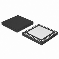
IC CTLR 8PH VR11.1 PMBUS 48-QFN
Manufacturer
ON Semiconductor
Datasheet
1.NCP4208MNR2G.pdf
(30 pages)
Specifications of NCP4208MNR2G
Applications
Controller, Intel VR11.1
Voltage - Input
4.7 ~ 5.75 V
Number Of Outputs
8
Voltage - Output
0.16 ~ 5 V
Operating Temperature
0°C ~ 85°C
Mounting Type
Surface Mount
Package / Case
48-TQFN Exposed Pad
Output Voltage
0.375 V to 1.6 V
Input Voltage
0.3 V to 6 V
Switching Frequency
1.5 MHz
Operating Temperature Range
0 C to + 85 C
Mounting Style
SMD/SMT
Duty Cycle (max)
100 %
Lead Free Status / RoHS Status
Lead free / RoHS Compliant
Available stocks
Company
Part Number
Manufacturer
Quantity
Price
Company:

Part Number:
NCP4208MNR2G
Manufacturer:
ON Semiconductor
Quantity:
1 200
Part Number:
NCP4208MNR2G
Manufacturer:
ON/安森美
Quantity:
20 000


ELECTRICAL CHARACTERISTICS
V
PSI
IMON
Current Limit Comparator
Current Balance Amplifier
Delay Timer
Soft−Start
Enable Input
ODN and OD1 Outputs
Power−Good Comparator
1. Performance guaranteed over the indicated operating temperature range by design and/or characterization tested at T
2. Refer to Application Information section.
3. Values based on design and/or characterization.
Input Low Voltage
Input High Voltage
Input Current
Assertion Timing
De−assertion Timing
Clamp Voltage
Accuracy
Output Current
Offset
I
Current Limit Threshold Current
Common−Mode Range
Input Resistance
Input Current
Input Current Matching
Phase Balance Adj. Range Low
Phase Balance Adj. Range High
Internal Timer
Timer Range Low
Timer Range High
Internal Timer
Timer Range Low
Timer Range High
Input Low Voltage
Input High Voltage
Input Current
Delay Time
Output Low Voltage
Output High Voltage
ODN / OD1 Pulldown Resistor
Undervoltage Threshold
Undervoltage Adj. Range Low
Undervoltage Adj. Range High
Overvoltage Threshold
LIM
IN
duty cycle pulse techniques are used during testing to maintain the junction temperature as close to ambient as possible.
= (5.0 V) FBRTN − GND, for typical values T
Bias Current
Parameter
Fsw = 300kHz
Fsw = 300kHz
10 x (CSREF − CSCOMP) / R
CSREF − CSCOMP / R
CSREF − CSCOMP = 150 mV, R
4/3 x I
SW(X) = 0 V
SW(X) = 0 V
SW(X) = 0 V
Phase Bal Registers = 00000
Phase Bal Registers = 11111
Delay Time Register = 011
Delay Time Register = 000
Delay Time Register = 111
Soft−Start Slope Register = 010
Soft−Start Slope Register = 000
Soft−Start Slope Register = 111
EN > 0.8 V, Internal Delay
I
I
Relative to Nominal DAC Output
PWRGD_LO Register = 000
PWRGD_LO Register = 111
Relative to DAC Output, PWRGD_Hi = 00
OD(SINK)
OD(SOURCE)
IREF
A
= −400 mA
= 25°C, for min/max values T
= 400 mA
Test Conditions
http://onsemi.com
ILIM
,
7
ILIM
ILIMC
= 7.5 kW
A
= 0°C to 85°C; unless otherwise noted. (Notes 1 and 2)
V
V
V
V
t
V
PWRGD(UV)
PWRGD(OV)
DELAY(EN)
Symbol
OL(ODN/1)
OL(ODN/1)
DI
R
V
SW(X)CM
V
I
I
IN(EN)
SW(X)
IH(EN)
I
SW(X)
IL(EN)
I
SW(X)
LIM
CL
−600
−600
−3.0
−6.0
−6.0
Min
200
0.8
1.0
7.0
0.8
4.0
14
−500
−500
−150
−5.0
−1.0
Typ
−25
+25
160
300
3.3
2.0
0.5
4.0
0.5
0.1
1.5
2.0
5.0
20
20
19
12
60
J
= T
+200
−400
Max
1.15
+6.0
A
825
800
500
400
0.3
3.0
6.0
0.3
25
20
= 25_C. Low
V/ms
V/ms
V/ms
Unit
mV
mV
mV
mV
mV
mV
mV
kW
ms
ms
ms
ms
kW
mA
mA
mA
mA
mA
mA
ms
ns
%
%
%
%
V
V
V
V
Related parts for NCP4208MNR2G
Image
Part Number
Description
Manufacturer
Datasheet
Request
R

Part Number:
Description:
VR11.1 Programmable 8-Phase Synchronous Buck Converter with PMBus
Manufacturer:
ONSEMI [ON Semiconductor]
Datasheet:

Part Number:
Description:
ON Semiconductor [VOLTAGE REGULATOR]
Manufacturer:
ON Semiconductor
Datasheet:
Part Number:
Description:
357-036-542-201 CARDEDGE 36POS DL .156 BLK LOPRO
Manufacturer:
ON Semiconductor
Datasheet:
Part Number:
Description:
357-036-542-201 CARDEDGE 36POS DL .156 BLK LOPRO
Manufacturer:
ON Semiconductor
Datasheet:
Part Number:
Description:
357-036-542-201 CARDEDGE 36POS DL .156 BLK LOPRO
Manufacturer:
ON Semiconductor
Datasheet:
Part Number:
Description:
357-036-542-201 CARDEDGE 36POS DL .156 BLK LOPRO
Manufacturer:
ON Semiconductor
Datasheet:
Part Number:
Description:
357-036-542-201 CARDEDGE 36POS DL .156 BLK LOPRO
Manufacturer:
ON Semiconductor
Datasheet:
Part Number:
Description:
357-036-542-201 CARDEDGE 36POS DL .156 BLK LOPRO
Manufacturer:
ON Semiconductor
Datasheet:
Part Number:
Description:
357-036-542-201 CARDEDGE 36POS DL .156 BLK LOPRO
Manufacturer:
ON Semiconductor
Datasheet:
Part Number:
Description:
357-036-542-201 CARDEDGE 36POS DL .156 BLK LOPRO
Manufacturer:
ON Semiconductor
Datasheet:
Part Number:
Description:
357-036-542-201 CARDEDGE 36POS DL .156 BLK LOPRO
Manufacturer:
ON Semiconductor
Datasheet:
Part Number:
Description:
357-036-542-201 CARDEDGE 36POS DL .156 BLK LOPRO
Manufacturer:
ON Semiconductor
Datasheet:
Part Number:
Description:
Manufacturer:
ON Semiconductor
Datasheet:
Part Number:
Description:
Manufacturer:
ON Semiconductor
Datasheet: