NCP4208MNR2G ON Semiconductor, NCP4208MNR2G Datasheet - Page 5
NCP4208MNR2G
Manufacturer Part Number
NCP4208MNR2G
Description
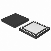
IC CTLR 8PH VR11.1 PMBUS 48-QFN
Manufacturer
ON Semiconductor
Datasheet
1.NCP4208MNR2G.pdf
(30 pages)
Specifications of NCP4208MNR2G
Applications
Controller, Intel VR11.1
Voltage - Input
4.7 ~ 5.75 V
Number Of Outputs
8
Voltage - Output
0.16 ~ 5 V
Operating Temperature
0°C ~ 85°C
Mounting Type
Surface Mount
Package / Case
48-TQFN Exposed Pad
Output Voltage
0.375 V to 1.6 V
Input Voltage
0.3 V to 6 V
Switching Frequency
1.5 MHz
Operating Temperature Range
0 C to + 85 C
Mounting Style
SMD/SMT
Duty Cycle (max)
100 %
Lead Free Status / RoHS Status
Lead free / RoHS Compliant
Available stocks
Company
Part Number
Manufacturer
Quantity
Price
Company:

Part Number:
NCP4208MNR2G
Manufacturer:
ON Semiconductor
Quantity:
1 200
Part Number:
NCP4208MNR2G
Manufacturer:
ON/安森美
Quantity:
20 000


PIN ASSIGNMENT
23 to 30
31 to 38
40 to 47
Pin No.
8 to 9
10
12
13
14
15
16
17
18
19
20
21
22
39
48
11
1
2
3
4
5
6
7
PWM8 to PWM1
VID7 to VID0
SW8 to SW1
Mnemonic
RAMPADJ
CSCOMP
PWRGD
CSSUM
FBRTN
CSREF
ALERT
ILIMFS
COMP
VCC3
IMON
IREF
GND
ODN
VCC
SDA
SCL
OD1
PSI
EN
NC
RT
FB
Power State Indicator. Pulling this pin low places the controller in lower power state operation.
3.3 V Power Supply Output. A capacitor from this pin to ground provided decoupling for the
interval 3.3 V LDO.
Power−Good Output: Open−drain output that signals when the output voltage is outside of the
proper operating range.
ALERT Output: Open drain output that asserts low when the VR exceeds a programmable limit.
Can be configured for Comparator Mode or Interrupt Mode.
Digital Input / Output. I
Digital Input. I
Power Supply Enable Input. Pulling this pin to GND disables the PWM outputs and pulls the
PWRGD output low.
Ground. All internal biasing and the logic output signals of the device are referenced to this
ground.
No Connect
Total Current Output Pin.
Current Reference Input. An external resistor from this pin to ground sets the reference current for
IFB, and IILIMFS.
Frequency Setting Resistor Input. An external resistor connected between this pin and GND
sets the oscillator frequency of the device.
PWM Ramp Current Input. An external resistor from the converter input voltage to this pin sets
the internal PWM ramp.
Feedback Return. VID DAC and error amplifier reference for remote sensing of the output
voltage.
Error Amplifier Output and Compensation Point.
Feedback Input. Error amplifier input for remote sensing of the output voltage. An external
resistor between this pin and the output voltage sets the no load offset point.
Current Sense Reference Voltage Input. The voltage on this pin is used as the reference for the
current sense amplifier and the power−good and crowbar functions. This pin should be
connected to the common point of the output inductors.
Current Sense Summing Node. External resistors from each switch node to this pin sum the
average inductor currents together to measure the total output current.
Current Sense Compensation Point. A resistor and capacitor from this pin to CSSUM
determines the gain of the current sense amplifier and the positioning loop response time.
Current Sense and Limit Scaling Pin. An external resistor from this pin to CSCOMP sets the
internal current sensing signal for current limit and IMON. This value can be overwritten using
the I
Output Disable Logic Output for PSI operation. This pin is actively pulled low when PSI is low,
otherwise it functions in the same way as OD1.
Output Disable Logic Output. This pin is actively pulled low when the EN input is low or when
VCC is below its UVLO threshold to signal to the Driver IC that the driver high−side and
low−side outputs should go low.
Current Balance Inputs. Inputs for measuring the current level in each phase. The SW pins of
unused phases should be left open.
Logic−Level PWM Outputs. Each output is connected to the input of an external MOSFET driver
such as the ADP3121. Connecting the PWM8, PWM7, PWM6, PWM5, PWM4, PWM3 and
PWM2 outputs to VCC causes that phase to turn off, allowing the NCP4208 to operate as a
1−, 2−, 3−, 4−, 5−, 6−, 7−, or 8−phase controller.
Supply Voltage for the Device. A 340 W resistor should be placed between the 12 V system
supply and the VCC pin. The internal shunt regulator maintains VCC = 5.0 V.
Voltage Identification DAC Inputs. These eight pins are pulled down to GND, providing a logic
zero if left open. When in normal operation mode, the DAC output programs the FB regulation
voltage from 0.375 V to 1.6 V.
2
C interface.
2
C serial bus clock open drain input. Requires pullup.
http://onsemi.com
2
C serial data bidirectional pin. Requires pullup.
5
Description
Related parts for NCP4208MNR2G
Image
Part Number
Description
Manufacturer
Datasheet
Request
R

Part Number:
Description:
VR11.1 Programmable 8-Phase Synchronous Buck Converter with PMBus
Manufacturer:
ONSEMI [ON Semiconductor]
Datasheet:

Part Number:
Description:
ON Semiconductor [VOLTAGE REGULATOR]
Manufacturer:
ON Semiconductor
Datasheet:
Part Number:
Description:
357-036-542-201 CARDEDGE 36POS DL .156 BLK LOPRO
Manufacturer:
ON Semiconductor
Datasheet:
Part Number:
Description:
357-036-542-201 CARDEDGE 36POS DL .156 BLK LOPRO
Manufacturer:
ON Semiconductor
Datasheet:
Part Number:
Description:
357-036-542-201 CARDEDGE 36POS DL .156 BLK LOPRO
Manufacturer:
ON Semiconductor
Datasheet:
Part Number:
Description:
357-036-542-201 CARDEDGE 36POS DL .156 BLK LOPRO
Manufacturer:
ON Semiconductor
Datasheet:
Part Number:
Description:
357-036-542-201 CARDEDGE 36POS DL .156 BLK LOPRO
Manufacturer:
ON Semiconductor
Datasheet:
Part Number:
Description:
357-036-542-201 CARDEDGE 36POS DL .156 BLK LOPRO
Manufacturer:
ON Semiconductor
Datasheet:
Part Number:
Description:
357-036-542-201 CARDEDGE 36POS DL .156 BLK LOPRO
Manufacturer:
ON Semiconductor
Datasheet:
Part Number:
Description:
357-036-542-201 CARDEDGE 36POS DL .156 BLK LOPRO
Manufacturer:
ON Semiconductor
Datasheet:
Part Number:
Description:
357-036-542-201 CARDEDGE 36POS DL .156 BLK LOPRO
Manufacturer:
ON Semiconductor
Datasheet:
Part Number:
Description:
357-036-542-201 CARDEDGE 36POS DL .156 BLK LOPRO
Manufacturer:
ON Semiconductor
Datasheet:
Part Number:
Description:
Manufacturer:
ON Semiconductor
Datasheet:
Part Number:
Description:
Manufacturer:
ON Semiconductor
Datasheet: