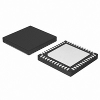
NCP4208MNR2G ON Semiconductor, NCP4208MNR2G Datasheet - Page 19

NCP4208MNR2G
Manufacturer Part Number
NCP4208MNR2G
Description
IC CTLR 8PH VR11.1 PMBUS 48-QFN
Manufacturer
ON Semiconductor
Datasheet
1.NCP4208MNR2G.pdf
(30 pages)
Specifications of NCP4208MNR2G
Applications
Controller, Intel VR11.1
Voltage - Input
4.7 ~ 5.75 V
Number Of Outputs
8
Voltage - Output
0.16 ~ 5 V
Operating Temperature
0°C ~ 85°C
Mounting Type
Surface Mount
Package / Case
48-TQFN Exposed Pad
Output Voltage
0.375 V to 1.6 V
Input Voltage
0.3 V to 6 V
Switching Frequency
1.5 MHz
Operating Temperature Range
0 C to + 85 C
Mounting Style
SMD/SMT
Duty Cycle (max)
100 %
Lead Free Status / RoHS Status
Lead free / RoHS Compliant
Available stocks
Company
Part Number
Manufacturer
Quantity
Price
Company:
Part Number:
NCP4208MNR2G
Manufacturer:
ON Semiconductor
Quantity:
1 200
Part Number:
NCP4208MNR2G
Manufacturer:
ON/安森美
Quantity:
20 000
Configuration Register 1 (0xD1)
Table 8. VR11 and VR10.x VID CODES for the NCP4208
Bit 3 BUS_TO_EN = 1; Bus timeout enabled.
10. The master asserts ACK on SDA.
12. After the last data byte the master asserts a No ACK
13. The master asserts a STOP condition on SDA.
11. The slave sends the remainder of the data byes, the
5. The master sends the 7−bit slave address followed
6. The slave asserts ACK on SDA.
7. The slave sends the byte count N.
8. The master asserts ACK on SDA.
9. The slave sends the first data byte.
by the read bit (high).
master asserts an ACK on SDA after each data byte.
on SDA.
OUTPUT
1.60000
1.59375
1.58750
1.58125
1.57500
1.56875
1.56250
1.55625
1.55000
1.54375
1.53750
1.53125
1.52500
1.51875
1.51250
1.50625
1.50000
1.49375
1.48750
1.48125
1.47500
1.46875
1.46250
1.45625
1.45000
1.44375
1.43750
1.43125
1.42500
1.41875
1.41250
1.40625
1.40000
OFF
OFF
VID7
0
0
0
0
0
0
0
0
0
0
0
0
0
0
0
0
0
0
0
0
0
0
0
0
0
0
0
0
0
0
0
0
0
0
0
VID6
0
0
0
0
0
0
0
0
0
0
0
0
0
0
0
0
0
0
0
0
0
0
0
0
0
0
0
0
0
0
0
0
0
0
0
http://onsemi.com
VID5
0
0
0
0
0
0
0
0
0
0
0
0
0
0
0
0
0
0
0
0
0
0
0
0
0
0
0
0
0
0
0
0
1
1
1
19
I
The NCP4208 includes a I
no I
bus is locked and releases the bus. This prevents the
device from locking or holding the I
The timeout feature can be disabled.
2
C Timeout
VID4
2
0
0
0
0
0
0
0
0
0
0
0
0
0
0
0
0
1
1
1
1
1
1
1
1
1
1
1
1
1
1
1
1
0
0
0
C activity for 35 ms, the NCP4208 assumes that the
Figure 20. Block Write to a Command Coder
S
1
ADDRESS
SLAVE
2
VID3
0
0
0
0
0
0
0
0
1
1
1
1
1
1
1
1
0
0
0
0
0
0
0
0
1
1
1
1
1
1
1
1
0
0
0
8
A
W
BYTE 1
DATA
3
A
9
S
ADDRESS
2
VID2
SLAVE
C timeout feature. If there is
10
4
A
0
0
0
0
1
1
1
1
0
0
0
0
1
1
1
1
0
0
0
0
1
1
1
1
0
0
0
0
1
1
1
1
0
0
0
...
5
R
2
6
A
C expecting data.
BYTE N
VID1
BYTE COUNT
DATA
0
0
1
1
0
0
1
1
0
0
1
1
0
0
1
1
0
0
1
1
0
0
1
1
0
0
1
1
0
0
1
1
0
0
1
11
7
= N
12
A
13
P
VID0
0
1
0
1
0
1
0
1
0
1
0
1
0
1
0
1
0
1
0
1
0
1
0
1
0
1
0
1
0
1
0
1
0
1
0


