ISL8112IRZ Intersil, ISL8112IRZ Datasheet - Page 8
ISL8112IRZ
Manufacturer Part Number
ISL8112IRZ
Description
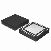
IC MAIN POWER SUPP CTRLR 32-QFN
Manufacturer
Intersil
Type
Step-Down (Buck)r
Datasheet
1.ISL8112IRZ.pdf
(27 pages)
Specifications of ISL8112IRZ
Internal Switch(s)
No
Synchronous Rectifier
Yes
Number Of Outputs
2
Voltage - Output
0.7 ~ 5.5 V
Current - Output
200mA
Voltage - Input
5.5 ~ 25 V
Operating Temperature
-40°C ~ 100°C
Mounting Type
Surface Mount
Package / Case
32-VQFN Exposed Pad, 32-HVQFN, 32-SQFN, 32-DHVQFN
Power - Output
5mW
Rohs Compliant
YES
Lead Free Status / RoHS Status
Lead free / RoHS Compliant
Frequency - Switching
-
Available stocks
Company
Part Number
Manufacturer
Quantity
Price
Company:

Part Number:
ISL8112IRZ
Manufacturer:
Intersil
Quantity:
315


Pin Descriptions
Typical Performance Curves
FIGURE 1. V
1.0
0.9
0.8
0.7
0.6
0.5
0.4
0.3
0.2
0.1
PIN
23
24
25
26
27
28
29
30
31
32
0
0.001
7 V
7 V
7 V
12 V
12 V
IN
IN
IN
IN
IN
OUT2REF Output voltage control for SMPS2. Connect OUT2REF to VCC for fixed 3.3V. Connect OUT2REF to VREF2 for fixed
PGOOD2
SKIP MODE
PWM MODE
ULTRA SKIP MODE
BOOT2
VSEN2
OUT2
MODE
NAME
SKIP MODE
PWM MODE
ILIM2
PH2
UG2
EN2
LG2
0.010
= 1.05V EFFICIENCY vs LOAD (300kHz)
(Continued)
SMPS2 Synchronous-Rectifier Gate-Drive Output. LG2 swings between GND and PVCC.
Boost Flying Capacitor Connection for SMPS2. Connect to an external capacitor according to the typical application
circuits (Figure 17 and Figure 18). See “MOSFET Gate Drivers (UG_, LG_)” on page 19.
Inductor Connection for SMPS2. PH2 is the internal lower supply rail for the UG2 high-side gate driver. PH2 is the
current-sense input for the SMPS2.
High-Side MOSFET Floating Gate-Driver Output for SMPS2. UG1 swings between PH2 and BOOT2.
SMPS2 Enable Input. The SMPS2 is enabled if EN2 is greater than the logic high level and disabled if EN2 is less than
the logic low level. If EN2 is connected to VREF1, the SMPS2 starts after the SMPS1 reaches regulation (delay start).
Drive EN2 below 0.8V to clear fault level and reset the fault latches.
SMP2 Power-Good Open-Drain Output. PGOOD2 is low when the SMPS2 output voltage is more than 10% below the
normal regulation point or during soft-start. PGOOD2 is high impedance when the output is in regulation and the soft-
start circuit has terminated. PGOOD2 is low in shutdown.
Low-Noise Mode Control. Connect MODE to GND for normal Idle-Mode (pulse-skipping) operation or to VCC for PWM
mode (fixed frequency). Connect to VREF1 or leave floating for ultrasonic skip mode operation.
SMPS2 Output Voltage-Sense Input. Connect to the SMPS2 output. VSEN2 is an input to the Constant on-time-PWM
on-time one-shot circuit. It also serves as the SMPS2 feedback input in fixed-voltage mode.
SMPS2 Current-Limit Adjustment. The GND-PH1 current-limit threshold is 1/10th the voltage seen at ILIM2 over a 0.2V
to 2V range. There is an internal 5µA current source from VCC to ILIM2. Connect ILIM2 to VREF1 for a fixed 200mV.
The logic current limit threshold is default to 100mV value if ILIM2 is higher than VCC - 1V.
1.05V. OUT2REF can be used to program SMPS2 output. VSEN2 equals OUT2REF from 0.5V to 2.50V. SMPS2 output
voltage is 0V if OUT2REF < 0.5V.
OUTPUT LOAD (A)
8
0.100
12 V
25 V
25 V
25 V
IN
IN
IN
IN
ULTRA SKIP MODE
SKIP MODE
PWM MODE
ULTRA SKIP MODE
Circuit of Figure 17 and Figure 18, no load on LDO, VSEN1, VSEN2, VREF2, and VREF1,
V
unless otherwise noted. Typical values are at T
IN
1.000
= 12V, EN2 = EN1 = VCC, VBYP = 5V, PVCC = 5V, VEN_LDO = 5V, T
10.000
ISL8112
FUNCTION
FIGURE 2. V
1.0
0.9
0.8
0.7
0.6
0.5
0.4
0.3
0.2
0.1
0
0.001
7 V
7 V
7 V
12 V
12 V
IN
IN
IN
IN
IN
A
SKIP MODE
PWM MODE
ULTRA SKIP MODE
OUT1
SKIP MODE
PWM MODE
= +25°C.
0.010
= 1.5V EFFICIENCY vs LOAD (200kHz)
OUTPUT LOAD (A)
0.100
12 V
25 V
25 V
25 V
A
IN
IN
IN
IN
= -40°C to +100°C,
ULTRA SKIP MODE
SKIP MODE
PWM MODE
ULTRA SKIP MODE
1.000
August 10, 2010
FN6396.1
10.000
Related parts for ISL8112IRZ
Image
Part Number
Description
Manufacturer
Datasheet
Request
R

Part Number:
Description:
Main Power Supply Controllers
Manufacturer:
Intersil Corporation
Datasheet:
Part Number:
Description:
Intersil Corporation [CMOS Serial Controller Interface]
Manufacturer:
Intersil Corporation
Datasheet:
Part Number:
Description:
Manufacturer:
Intersil Corporation
Datasheet:
Part Number:
Description:
357-036-542-201 CARDEDGE 36POS DL .156 BLK LOPRO
Manufacturer:
Intersil Corporation
Datasheet:
Part Number:
Description:
1024-Word x 4-Bit LSI Static RAM
Manufacturer:
Intersil Corporation
Datasheet:
Part Number:
Description:
General Purpose NPN Transistor Arrays FN341.4
Manufacturer:
Intersil Corporation
Datasheet:
Part Number:
Description:
CMOS 16-Bit Microprocessor
Manufacturer:
Intersil Corporation
Datasheet:
Part Number:
Description:
Manufacturer:
Intersil Corporation
Datasheet:
Part Number:
Description:
Manufacturer:
Intersil Corporation
Datasheet:
Part Number:
Description:
Manufacturer:
Intersil Corporation
Datasheet:
Part Number:
Description:
Manufacturer:
Intersil Corporation
Datasheet:
Part Number:
Description:
CMOS 6-Bit Latch and Decoder Memory Interfaces
Manufacturer:
Intersil Corporation
Datasheet:
Part Number:
Description:
CA3046General Purpose NPN Transistor Arrays
Manufacturer:
Intersil Corporation
Datasheet:
Part Number:
Description:
Manufacturer:
Intersil Corporation
Datasheet:
Part Number:
Description:
TR909 DLC/FLC SLIC with Low Power Standby
Manufacturer:
Intersil Corporation
Datasheet: