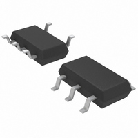
LTC1701ES5#TR Linear Technology, LTC1701ES5#TR Datasheet - Page 4

LTC1701ES5#TR
Manufacturer Part Number
LTC1701ES5#TR
Description
IC CONV DC/DC STEP DOWN TSOT23-5
Manufacturer
Linear Technology
Type
Step-Down (Buck)r
Datasheet
1.LTC1701BES5TRM.pdf
(12 pages)
Specifications of LTC1701ES5#TR
Internal Switch(s)
Yes
Synchronous Rectifier
No
Number Of Outputs
1
Voltage - Output
1.25 ~ 5 V
Current - Output
500mA
Frequency - Switching
1MHz
Voltage - Input
2.5 ~ 5.5 V
Operating Temperature
-40°C ~ 85°C
Mounting Type
Surface Mount
Package / Case
TSOT-23-5, TSOT-5, TSOP-5
Lead Free Status / RoHS Status
Contains lead / RoHS non-compliant
Power - Output
-
Available stocks
Company
Part Number
Manufacturer
Quantity
Price
PI FU CTIO S
LTC1701/LTC1701B
SW (Pin 1): The Switch Node Connection to the Inductor.
This pin swings from V
voltage drop below ground. The cathode of the Schottky
diode must be closely connected to this pin.
GND (Pin 2): Ground Pin. Connect to the (–) terminal of
C
V
external resistive divider across the output. Nominal volt-
age for this pin is 1.25V.
Pin Limit Table
PIN
1
2
3
4
5
BLOCK DIAGRA
4
I
OUT
FB
TH
U
/RUN
V
(Pin 3): Receives the feedback voltage from the
, the Schottky diode and (–) terminal of C
FB
V
V
REF
REF
U
NAME
SW
GND
V
I
V
TH
FB
IN
/RUN
–
–
+
+
ERROR
1.4V
I
CLAMP
TH
AMP
/REF
U
+
–
VOLTAGE
COMP
IN
OVER
to a Schottky diode (external)
W
DESCRIPTION
Switch Node
Ground Pin
Output Feedback Pin
Error Amplifier Compensation and RUN Pin
Main Power Supply
V
IN
50 A
(1.25V TO 2.25V)
SHDN
STRETCHER
V
FB
PULSE
< 0.6V
IN
1.5V
.
REFERENCE
BANDGAP
1.25V
V
IN
–
+
(LTC1701 only)
COMP
I
TH
I
sation Point and Run Control Input. The current compara-
tor threshold increases with this control voltage. Nominal
voltage range for this pin is 1.25V to 2.25V. Forcing this
pin below 0.8V causes the device to be shut down. In
shutdown all functions are disabled.
V
Current Comparator. Must be closely decoupled to ground.
TH
IN
/RUN (Pin 4): Combination of Error Amplifier Compen-
(Pin 5): Main Supply Pin and the (+) Input to the
V
(1.25V)
REF
– 0.3
MIN
2.5
0
0
NOMINAL (V)
CURRENT
COMP
1.25
TYP
0
+
–
CONTROL LOGIC
OFF-TIMER
V
AND GATE
MAX
1.35
2.25
V
5.5
REF
IN
V
IN
– 0.3
– 0.3
– 0.3
MIN
– 8.5
ABSOLUTE MAX (V)
CURRENT
SENSE
AMP
DRIVER
GATE
–
+
GND
V
V
IN
IN
MAX
+ 0.3
3
3
6
1701 BD
SW


