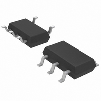
LTC1701ES5#TR Linear Technology, LTC1701ES5#TR Datasheet - Page 9

LTC1701ES5#TR
Manufacturer Part Number
LTC1701ES5#TR
Description
IC CONV DC/DC STEP DOWN TSOT23-5
Manufacturer
Linear Technology
Type
Step-Down (Buck)r
Datasheet
1.LTC1701BES5TRM.pdf
(12 pages)
Specifications of LTC1701ES5#TR
Internal Switch(s)
Yes
Synchronous Rectifier
No
Number Of Outputs
1
Voltage - Output
1.25 ~ 5 V
Current - Output
500mA
Frequency - Switching
1MHz
Voltage - Input
2.5 ~ 5.5 V
Operating Temperature
-40°C ~ 85°C
Mounting Type
Surface Mount
Package / Case
TSOT-23-5, TSOT-5, TSOP-5
Lead Free Status / RoHS Status
Contains lead / RoHS non-compliant
Power - Output
-
Available stocks
Company
Part Number
Manufacturer
Quantity
Price
APPLICATIO S I FOR ATIO
During normal operation the voltage on the I
will vary from 1.25V to 2.25V depending on the load
current. Pulling the I
LTC1701 into a low quiescent current shutdown mode
(I
shown in Figures 3(a).
Efficiency Considerations
The percent efficiency of a switching regulator is equal to
the output power divided by the input power times 100%.
It is often useful to analyze individual losses to determine
what is limiting the efficiency and what change would
produce the most improvement. Percent efficiency can be
expressed as:
where L1, L2, etc. are the individual losses as a percentage
of input power.
Although all dissipative elements in the circuit produce
losses, 4 main sources usually account for most of the
losses in LTC1701 circuits: 1) LTC1701 V
2) switching losses, 3) I
losses.
1) The V
electrical characteristics which excludes MOSFET driver
and control currents. V
loss that increases with V
2) The switching current is the sum of the internal MOSFET
driver and control currents. The MOSFET driver current
results from switching the gate capacitance of the power
MOSFET. Each time a MOSFET gate is switched from low
to high to low again, a packet of charge dQ moves from V
to ground. The resulting dQ/dt is a current out of V
is typically much larger than the control circuit current. In
Q
%Efficiency = 100% – (L1 + L2 + L3 + ...)
< 1 A). This pin can be driven directly from logic as
IN
(a)
current is the DC supply current given in the
I
TH
/RUN
Figure 3. I
R
C
C
C
U
TH
IN
TH
current results in a small (< 0.1%)
/RUN pin below 0.8V puts the
/RUN Pin Interfacing
2
IN
U
R losses, 4) Schottky diode
, even at no load.
W
R1
(b)
C1
D1
I
TH
TH
IN
/RUN
U
/RUN pin
1701 F03
current,
R
C
C
IN
C
that
IN
continuous mode, I
charge of the internal MOSFET switch.
3) I
MOSFET and inductor. In continuous mode the average
output current flows through L, but is “chopped” between
the topside internal MOSFET and the Schottky diode. At
low supply voltages where the switch on-resistance is
higher and the switch is on for longer periods due to the
higher duty cycle, the switch losses will dominate. Using
a larger inductance helps minimize these switch losses. At
high supply voltages, these losses are proportional to the
load. I
currents.
4) The Schottky diode is a major source of power loss at
high currents and gets worse at low output voltages. The
diode loss is calculated by multiplying the forward voltage
drop times the diode duty cycle multiplied by the load
current.
Other “hidden” losses such as copper trace and internal
battery resistances can account for additional efficiency
degradations in portable systems. It is very important to
include these “system” level losses in the design of a
system. The internal battery and fuse resistance losses
can be minimized by making sure that C
charge storage and very low ESR at the switching fre-
quency. Other losses including Schottky conduction losses
during dead-time and inductor core losses generally ac-
count for less than 2% total additional loss.
THERMAL CONSIDERATIONS
The power handling capability of the device at high ambi-
ent temperatures will be limited by the maximum rated
junction temperature (125 C). It is important to give
careful consideration to all sources of thermal resistance
from junction to ambient. Additional heat sources mounted
nearby must also be considered.
For surface mount devices, heat sinking is accomplished
by using the heat spreading capabilities of the PC board
and its copper traces. Copper board stiffeners and plated
through-holes can also be used to spread the heat gener-
ated by power devices.
2
R Losses are predicted from the DC resistances of the
2
R losses cause the efficiency to drop at high output
LTC1701/LTC1701B
GATECHG
= f • Q
P
, where Q
IN
has adequate
P
is the gate
9


