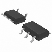
LTC1701ES5#TR Linear Technology, LTC1701ES5#TR Datasheet - Page 8

LTC1701ES5#TR
Manufacturer Part Number
LTC1701ES5#TR
Description
IC CONV DC/DC STEP DOWN TSOT23-5
Manufacturer
Linear Technology
Type
Step-Down (Buck)r
Datasheet
1.LTC1701BES5TRM.pdf
(12 pages)
Specifications of LTC1701ES5#TR
Internal Switch(s)
Yes
Synchronous Rectifier
No
Number Of Outputs
1
Voltage - Output
1.25 ~ 5 V
Current - Output
500mA
Frequency - Switching
1MHz
Voltage - Input
2.5 ~ 5.5 V
Operating Temperature
-40°C ~ 85°C
Mounting Type
Surface Mount
Package / Case
TSOT-23-5, TSOT-5, TSOP-5
Lead Free Status / RoHS Status
Contains lead / RoHS non-compliant
Power - Output
-
Available stocks
Company
Part Number
Manufacturer
Quantity
Price
LTC1701/LTC1701B
APPLICATIO S I FOR ATIO
Figure 2. The output voltage is set by a resistive divider
according to the following formula:
To prevent stray pickup, a capacitor of about 5pF can be
added across R1, located close to the LTC1701. Unfortu-
nately, the load step response is degraded by this capaci-
tor. Using a good printed circuit board layout eliminates
the need for this capacitor. Great care should be taken to
route the V
inductor or the SW line.
Transient Response
The OPTI-LOOP compensation allows the transient re-
sponse to be optimized for a wide range of loads and
output capacitors. The availability of the I
allows optimization of the control loop behavior but also
provides a DC coupled and AC filtered closed-loop re-
sponse test point. The DC step, rise time and settling at this
test point truly reflects the closed-loop response. Assum-
ing a predominately second order system, phase margin
and/or damping factor can be estimated using the percent-
age of overshoot seen at this pin. The bandwidth can also
be estimated by examining the rise time at the pin.
The I
will provide an adequate starting point for most applica-
tions. The series R3-C3 filter sets the dominant pole-zero
loop compensation. The values can be modified slightly
(from 0.5 to 2 times their suggested values) to optimize
transient response once the final PC layout is done and the
particular output capacitor type and value have been
determined. The output capacitors need to be selected
because the various types and values determine the loop
feedback factor gain and phrase. An output current pulse
8
V
OUT
TH
external components shown in the Figure 1 circuit
= 1.25V(1 + R2/R1)
FB
Figure 2. Setting the Output Voltage
line away from noise sources, such as the
LTC1701
SGND
U
V
FB
U
5pF
C
W
F
V
OUT
R2
1%
R1
1%
1701 F02
TH
pin not only
U
of 20% to 100% of full-load current having a rise time of
1 s to 10 s will produce output voltage and I
waveforms that will give a sense of the overall loop
stability without breaking the feedback loop.
The initial output voltage step may not be within the
bandwidth of the feedback loop, so the standard second-
order overshoot/DC ratio cannot be used to determine
phase margin. The gain of the loop increases with R3 and
the bandwidth of the loop increases with decreasing C3. If
R3 is increased by the same factor that C3 is decreased,
the zero frequency will be kept the same, thereby keeping
the phase the same in the most critical frequency range of
the feedback loop. In addition, a feed-forward capacitor,
C
as shown in Figure 2. Capacitor C
creating a high frequency zero with R2 which improves the
phase margin.
The output voltage settling behavior is related to the
stability of the closed-loop system and will demonstrate
the actual overall supply performance. For a detailed
explanation of optimizing the compensation components,
including a review of control loop theory, refer to Applica-
tion Note 76.
RUN Function
The I
loop compensation and a means to shut down the LTC1701.
Soft-start can also be implemented with this pin. Soft-start
reduces surge currents from V
the internal peak inductor current. Power supply sequenc-
ing can also be accomplished using this pin.
An external pull-up is required to charge the external
capacitor C3 in Figure 1. Typically, a 1M resistor between
V
reaches about 0.8V the LTC1701 begins operating. At this
point the error amplifier pulls up the I
normal operating range of 1.25V to 2.25V.
Soft-start can be implemented by ramping the voltage on
I
voltage on I
internal peak current limit is also ramped at a proportional
linear rate.
TH
F
IN
, can be added to improve the high frequency response,
/RUN during start-up as shown in Figure 3(b). As the
and I
TH
/RUN pin is a dual purpose pin that provides the
TH
/RUN is used. When the voltage on I
TH
/RUN ramps through its operating range the
IN
F
by gradually increasing
provides phase lead by
TH
/RUN pin to the
TH
TH
/RUN
pin


