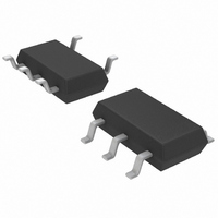
LTC1701ES5#TR Linear Technology, LTC1701ES5#TR Datasheet - Page 5

LTC1701ES5#TR
Manufacturer Part Number
LTC1701ES5#TR
Description
IC CONV DC/DC STEP DOWN TSOT23-5
Manufacturer
Linear Technology
Type
Step-Down (Buck)r
Datasheet
1.LTC1701BES5TRM.pdf
(12 pages)
Specifications of LTC1701ES5#TR
Internal Switch(s)
Yes
Synchronous Rectifier
No
Number Of Outputs
1
Voltage - Output
1.25 ~ 5 V
Current - Output
500mA
Frequency - Switching
1MHz
Voltage - Input
2.5 ~ 5.5 V
Operating Temperature
-40°C ~ 85°C
Mounting Type
Surface Mount
Package / Case
TSOT-23-5, TSOT-5, TSOP-5
Lead Free Status / RoHS Status
Contains lead / RoHS non-compliant
Power - Output
-
Available stocks
Company
Part Number
Manufacturer
Quantity
Price
OPERATIO
The LTC1701 uses a contant off-time, current mode archi-
tecture. The operating frequency is then determined by the
off-time and the difference between V
The output voltage is set by an external divider returned to
the V
voltage with a reference voltage of 1.25V and adjusts the
peak inductor current accordingly.
Main Control Loop
During normal operation, the internal PMOS switch is
turned on when the V
voltage. The current into the inductor and the load in-
creases until the current limit is reached. The switch turns
off and energy stored in the inductor flows through the
external Schottky diode into the load. After the constant
off-time interval, the switch turns on and the cycle repeats.
The peak inductor current is controlled by the voltage on
the I
amplifier.This amplifier compares the V
reference. When the load current increases, the FB voltage
decreases slightly below the reference. This decrease
causes the error amplifier to increase the I
until the average inductor current matches the new load
current.
The main control loop is shut down by pulling the I
pin to ground. When the pin is released an external resistor
is used to charge the compensation capacitor. When the
voltage at the I
APPLICATIO S I FOR ATIO
The basic LTC1701 application circuit is shown in
Figure 1. External component selection is driven by the
load requirement and begins with the selection of L1. Once
L1 is chosen, the Schottky diode D1 can be selected
followed by C
L Selection and Operating Frequency
The operating frequency is fixed by V
constant off-time of about 500ns. The complete expres-
sion for operating frequency is given by:
FB
TH
pin. An error amplfier compares the divided output
/RUN pin, which is the output of the error
IN
TH
and C
/RUN pin reaches 0.8V, the main control
U
U
OUT
FB
.
voltage is below the reference
U
W
IN
FB
IN
and V
pin to the 1.25V
TH
, V
/RUN voltage
OUT
OUT
U
TH
and the
.
/RUN
loop is enabled and the error amplifier drives the I
pin. Soft-start can be implemented by ramping the voltage
on the I
tion).
Low Current Operation
To optimize efficiency when the load is relatively light, the
LTC1701 automatically switches to Burst Mode operation
in which the internal PMOS switch operates intermittently
based on load demand. The main control loop is inter-
rupted when the output voltage reaches the desired regu-
lated value. The hysteretic voltage comparator trips when
I
ing the power consumed. The output capacitor and the
inductor supply the power to the load until the output
voltage drops slightly and the I
turning on the switch and the main control loop which
starts another cycle.
For reduced output ripple, the LTC1701B doesn't use
Burst Mode operation and operates continuously down to
very low currents where the part starts skipping cycles.
Dropout Operation
In dropout, the internal PMOS switch is turned on continu-
ously (100% duty cycle) providing low dropout operation
with V
an under voltage lockout, care should be taken to shut
down the LTC1701 for V
Although the inductor does not influence the operating
frequency, the inductor value has a direct effect on ripple
current. The inductor ripple current I
higher inductance and increases with higher V
where V
TH
/RUN is below 1.5V, shutting off the switch and reduc-
f
O
I
L
OUT
D
TH
V
is the output Schottky diode forward drop.
at V
IN
/RUN pin (see Applications Information sec-
V
V
IN
IN
IN
V
fL
. Since the LTC1701 does not incorporate
OUT
V
V
D
LTC1701/LTC1701B
OUT
T
IN
OFF
V
1
V
OUT
< 2.5V.
IN
TH
V
V
D
/RUN pin exceeds 1.5V,
D
L
decreases with
IN
or V
TH
/RUN
OUT
5
:


