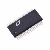
LTC1709EG-8 Linear Technology, LTC1709EG-8 Datasheet - Page 11

LTC1709EG-8
Manufacturer Part Number
LTC1709EG-8
Description
IC REG SW 2PH SYNC STPDWN 36SSOP
Manufacturer
Linear Technology
Type
Step-Down (Buck)r
Datasheet
1.LTC1709EG-8PBF.pdf
(28 pages)
Specifications of LTC1709EG-8
Internal Switch(s)
No
Synchronous Rectifier
Yes
Number Of Outputs
2
Voltage - Output
1.3 ~ 3.5 V
Current - Output
3A
Voltage - Input
4 ~ 36 V
Operating Temperature
-40°C ~ 85°C
Mounting Type
Surface Mount
Package / Case
36-SSOP
Lead Free Status / RoHS Status
Contains lead / RoHS non-compliant
Power - Output
-
Frequency - Switching
-
Available stocks
Company
Part Number
Manufacturer
Quantity
Price
Part Number:
LTC1709EG-8
Manufacturer:
LT/凌特
Quantity:
20 000
Company:
Part Number:
LTC1709EG-85
Manufacturer:
LT
Quantity:
389
Part Number:
LTC1709EG-85
Manufacturer:
LT/凌特
Quantity:
20 000
Part Number:
LTC1709EG-85#TR
Manufacturer:
LT/凌特
Quantity:
20 000
OPERATIO
Differential Amplifier
This amplifier provides true differential output voltage
sensing. Sensing both V
tion in high current applications and/or applications hav-
ing electrical interconnection losses. The AMPMD pin
allows selection of internal, precision feedback resistors
for high common mode rejection differencing applica-
tions, or direct access to the actual amplifier inputs
without these internal feedback resistors for other applica-
tions. The AMPMD pin is grounded to connect the internal
precision resistors in a unity-gain differencing application,
or tied to the INTV
and make the amplifier inputs directly available. The
amplifier is a unity-gain stable, 2MHz gain bandwidth,
>120dB open-loop gain design. The amplifier has an
output slew rate of 5V/ s and is capable of driving capaci-
tive loads with an output RMS current typically up to
35mA. The amplifier is not capable of sinking current and
therefore must be resistively loaded to do so.
Power Good (PGOOD)
The PGOOD pin is connected to the drain of an internal
MOSFET. The MOSFET turns on when the output voltage
is not within 7.5% of its nominal output level as deter-
mined by the feedback divider. When the output is within
APPLICATIO S I FOR ATIO
The basic LTC1709 application circuit is shown in Fig-
ure 1 on the first page. External component selection
begins with the selection of the inductor(s) based on
ripple current requirements and continues with the
R
inductor current and/or maximum current limit. Next, the
power MOSFETs and D1 and D2 are selected. The oper-
ating frequency and the inductor are chosen based mainly
on the amount of ripple current. Finally, C
its ability to handle the input ripple current (that
PolyPhase
with low enough ESR to meet the output ripple voltage
and load step specifications (also minimized with
PolyPhase). Current mode architecture provides inherent
SENSE1, 2
TM
resistor selection using the calculated peak
operation minimizes) and C
U
CC
U
pin to bypass the internal resistors
(Refer to Functional Diagram)
OUT
U
+
and V
OUT
W
–
IN
benefits regula-
OUT
is selected for
is chosen
U
within 10 s and the PGOOD pin should be pulled up by an
external resistor to a source of up to 7V.
Short-Circuit Detection
The RUN/SS capacitor is used initially to limit the inrush
current from the input power source. Once the controllers
have been given time, as determined by the capacitor on
the RUN/SS pin, to charge up the output capacitors and
provide full-load current, the RUN/SS capacitor is then
used as a short-circuit timeout circuit. If the output voltage
falls to less than 70% of its nominal output voltage the
RUN/SS capacitor begins discharging assuming that the
output is in a severe overcurrent and/or short-circuit
condition. If the condition lasts for a long enough period
as determined by the size of the RUN/SS capacitor, the
controller will be shut down until the RUN/SS pin voltage
is recycled. This built-in latchoff can be overidden by
providing a current >5 A at a compliance of 5V to the
RUN/SS pin. This current shortens the soft-start period
but also prevents net discharge of the RUN/SS capacitor
during a severe overcurrent and/or short-circuit condi-
tion. Foldback current limiting is activated when the output
voltage falls below 70% of its nominal level whether or not
the short-circuit latchoff circuit is enabled.
current sharing between output stages. The circuit shown
in Figure 1 can be configured for operation up to an input
voltage of 28V (limited by the external MOSFETs).
R
R
current. The LTC1709 current comparator has a maxi-
mum threshold of 75mV/R
mode range of SGND to 1.1(INTV
parator threshold sets the peak inductor current, yielding
a maximum average output current I
value less half the peak-to-peak ripple current, I
PolyPhase is a trademark of Linear Technology Corporation.
7.5% of its nominal value, the MOSFET is turned off
SENSE
SENSE1, 2
Selection For Output Current
are chosen based on the required peak output
LTC1709-8/LTC1709-9
SENSE
and an input common
CC
MAX
). The current com-
equal to the peak
11
L
.


