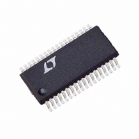
LTC1709EG-8 Linear Technology, LTC1709EG-8 Datasheet - Page 17

LTC1709EG-8
Manufacturer Part Number
LTC1709EG-8
Description
IC REG SW 2PH SYNC STPDWN 36SSOP
Manufacturer
Linear Technology
Type
Step-Down (Buck)r
Datasheet
1.LTC1709EG-8PBF.pdf
(28 pages)
Specifications of LTC1709EG-8
Internal Switch(s)
No
Synchronous Rectifier
Yes
Number Of Outputs
2
Voltage - Output
1.3 ~ 3.5 V
Current - Output
3A
Voltage - Input
4 ~ 36 V
Operating Temperature
-40°C ~ 85°C
Mounting Type
Surface Mount
Package / Case
36-SSOP
Lead Free Status / RoHS Status
Contains lead / RoHS non-compliant
Power - Output
-
Frequency - Switching
-
Available stocks
Company
Part Number
Manufacturer
Quantity
Price
Part Number:
LTC1709EG-8
Manufacturer:
LT/凌特
Quantity:
20 000
Company:
Part Number:
LTC1709EG-85
Manufacturer:
LT
Quantity:
389
Part Number:
LTC1709EG-85
Manufacturer:
LT/凌特
Quantity:
20 000
Part Number:
LTC1709EG-85#TR
Manufacturer:
LT/凌特
Quantity:
20 000
APPLICATIO S I FOR ATIO
INTV
turns on, the driver places the C
source of the desired MOSFET. This enhances the MOSFET
and turns on the topside switch. The switch node voltage,
SW, rises to V
The value of the boost capacitor C
times that of the total input capacitance of the topside
MOSFET(s). The reverse breakdown of D
than V
The final arbiter when defining the best gate drive ampli-
tude level will be the input supply current. If a change is
made that decreases input current, the efficiency has
improved. If the input current does not change then the
efficiency has not changed either.
Output Voltage
The LTC1709 has a true remote voltage sense capablity.
The sensing connections should be returned from the load
back to the differential amplifier’s inputs through a com-
mon, tightly coupled pair of PC traces. The differential
amplifier corrects for DC drops in both the power and
ground paths. The differential amplifier output signal is
divided down and compared with the internal precision
0.8V voltage reference by the error amplifier.
Output Voltage Programming
The output voltage is digitally programmed as defined in
Table 1 using the VID0 to VID4 logic input pins. The VID
logic inputs program a precision, 0.25% internal feedback
resistive divider. The LTC1709-8 has an output voltage
range of 1.30V to 3.5V in 50mV and 100mV steps. The
LTC1709-9 has an output voltage range of 1.10V to 1.85V
in 25mV steps.
Between the ATTENOUT pin and ground is a variable
resistor, R1, whose value is controlled by the five VID input
pins (VID0 to VID4). Another resistor, R2, between the
ATTENIN and the ATTENOUT pins completes the resistive
divider. The output voltage is thus set by the ratio of
(R1 + R2) to R1.
CC
IN(MAX).
when the SW pin is low. When the topside MOSFET
IN
and the BOOST pin rises to V
U
U
B
voltage across the gate-
B
needs to be 30 to 100
W
B
must be greater
IN
+ V
U
INTVCC
.
Table 1. VID Output Voltage Programming
*Represents codes without a defined output voltage as specified in Intel
specifications. The LTC1709 interprets these codes as a valid input and
produces an output voltage as follows:
VID4
0
0
0
0
0
0
0
0
0
0
0
0
0
0
0
0
1
1
1
1
1
1
1
1
1
1
1
1
1
1
1
1
LTC1709-8 (11111) = 2V
LTC1709-9 (11111) = 1.075V
VID3
0
0
0
0
0
0
0
0
1
1
1
1
1
1
1
1
0
0
0
0
0
0
0
0
1
1
1
1
1
1
1
1
VID2
0
0
0
0
1
1
1
1
0
0
0
0
1
1
1
1
0
0
0
0
1
1
1
1
0
0
0
0
1
1
1
1
LTC1709-8/LTC1709-9
VID1
0
0
1
1
0
0
1
1
0
0
1
1
0
0
1
1
0
0
1
1
0
0
1
1
0
0
1
1
0
0
1
1
VID0
0
1
0
1
0
1
0
1
0
1
0
1
0
1
0
1
0
1
0
1
0
1
0
1
0
1
0
1
0
1
0
1
Shutdown*
LTC1709-8
No_CPU/
VRM8.4
2.05V
2.00V
1.95V
1.90V
1.85V
1.80V
1.75V
1.70V
1.65V
1.60V
1.55V
1.50V
1.45V
1.40V
1.35V
1.30V
3.50V
3.40V
3.30V
3.20V
3.10V
3.00V
2.90V
2.80V
2.70V
2.60V
2.50V
2.40V
2.30V
2.20V
2.10V
LTC1709-9
Shutdown*
No_CPU/
VRM9.0
1.850V
1.825V
1.800V
1.775V
1.750V
1.725V
1.700V
1.675V
1.650V
1.625V
1.600V
1.575V
1.550V
1.525V
1.500V
1.475V
1.450V
1.425V
1.400V
1.375V
1.350V
1.325V
1.300V
1.275V
1.250V
1.225V
1.200V
1.175V
1.150V
1.125V
1.100V
17


