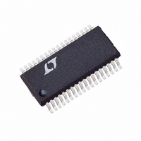
LTC1709EG-8 Linear Technology, LTC1709EG-8 Datasheet - Page 20

LTC1709EG-8
Manufacturer Part Number
LTC1709EG-8
Description
IC REG SW 2PH SYNC STPDWN 36SSOP
Manufacturer
Linear Technology
Type
Step-Down (Buck)r
Datasheet
1.LTC1709EG-8PBF.pdf
(28 pages)
Specifications of LTC1709EG-8
Internal Switch(s)
No
Synchronous Rectifier
Yes
Number Of Outputs
2
Voltage - Output
1.3 ~ 3.5 V
Current - Output
3A
Voltage - Input
4 ~ 36 V
Operating Temperature
-40°C ~ 85°C
Mounting Type
Surface Mount
Package / Case
36-SSOP
Lead Free Status / RoHS Status
Contains lead / RoHS non-compliant
Power - Output
-
Frequency - Switching
-
Available stocks
Company
Part Number
Manufacturer
Quantity
Price
Part Number:
LTC1709EG-8
Manufacturer:
LT/凌特
Quantity:
20 000
Company:
Part Number:
LTC1709EG-85
Manufacturer:
LT
Quantity:
389
Part Number:
LTC1709EG-85
Manufacturer:
LT/凌特
Quantity:
20 000
Part Number:
LTC1709EG-85#TR
Manufacturer:
LT/凌特
Quantity:
20 000
APPLICATIO S I FOR ATIO
LTC1709-8/LTC1709-9
The loop filter components (C
current pulses from the phase detector and provide a
stable input to the voltage controlled oscillator. The filter
components C
acquires lock. Typically R
0.1 F.
Minimum On-Time Considerations
Minimum on-time, t
that the LTC1709 is capable of turning on the top MOSFET.
It is determined by internal timing delays and the gate
charge required to turn on the top MOSFET. Low duty cycle
applications may approach this minimum on-time limit
and care should be taken to ensure that:
If the duty cycle falls below what can be accommodated by
the minimum on-time, the LTC1709 will begin to skip
cycles resulting in variable frequency operation. The out-
put voltage will continue to be regulated, but the ripple
current and ripple voltage will increase.
The minimum on-time for the LTC1709 is generally less
than 200ns. However, as the peak sense voltage de-
creases, the minimum on-time gradually increases. This is
of particular concern in forced continuous applications
with low ripple current at light loads. If the duty cycle drops
below the minimum on-time limit in this situation, a
significant amount of cycle skipping can occur with corre-
spondingly larger ripple current and voltage ripple.
If an application can operate close to the minimum
on-time limit, an inductor must be chosen that has a low
enough inductance to provide sufficient ripple amplitude
to meet the minimum on-time requirement. As a general
rule, keep the inductor ripple current of each phase equal
to or greater than 15% of I
Voltage Positioning
Voltage positioning can be used to minimize peak-to-peak
output voltage excursion under worst-case transient load-
ing conditions. The open-loop DC gain of the control loop
20
t
ON MIN
V f
LP
V
IN
OUT
and R
U
ON(MIN)
LP
U
LP
, is the smallest time duration
determine how fast the loop
OUT(MAX)
=10k and C
LP
, R
W
LP
at V
) smooth out the
IN(MAX)
LP
is 0.01 F to
U
.
is reduced depending upon the maximum load step speci-
fications. Voltage positioning can easily be added to the
LTC1709 by loading the I
having a Thevenin equivalent voltage source equal to the
midpoint operating voltage of the error amplifier, or 1.2V
(see Figure 8).
The resistive load reduces the DC loop gain while main-
taining the linear control range of the error amplifier. The
worst-case peak-to-peak output voltage deviation due to
transient loading can theoretically be reduced to half or
alternatively the amount of output capacitance can be
reduced for a particular application. A complete explana-
tion is included in Design Solutions 10 or the LTC1736
data sheet. (See www.linear-tech.com)
Efficiency Considerations
The percent efficiency of a switching regulator is equal to
the output power divided by the input power times 100%.
It is often useful to analyze individual losses to determine
what is limiting the efficiency and which change would
produce the most improvement. Percent efficiency can be
expressed as:
where L1, L2, etc. are the individual losses as a percentage
of input power.
Although all dissipative elements in the circuit produce
losses, four main sources usually account for most of the
losses in LTC1709 circuits: 1) I
MOSFET transition losses, 3) INTV
and 4) LTC1709 V
differential amplifier output).
Figure 8. Active Voltage Positioning Applied to the LTC1709
%Efficiency = 100% – (L1 + L2 + L3 + ...)
INTV
CC
R
R
T2
T1
IN
current (including loading on the
R
C
C
C
TH
I
pin with a resistive divider
TH
LTC1709
2
R losses, 2) Topside
CC
1709 F08
regulator current


