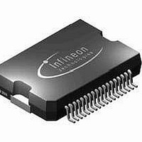
TLE6361G Infineon Technologies, TLE6361G Datasheet - Page 10

TLE6361G
Manufacturer Part Number
TLE6361G
Description
IC PS SYSTEM MULTI VOLT PDSO-36
Manufacturer
Infineon Technologies
Type
Step-Down (Buck)r
Datasheet
1.TLE6361G.pdf
(57 pages)
Specifications of TLE6361G
Internal Switch(s)
Yes
Synchronous Rectifier
No
Number Of Outputs
4
Voltage - Output
5.4 ~ 6.05 V
Current - Output
1.5A
Frequency - Switching
370kHz
Voltage - Input
5.5 ~ 60 V
Operating Temperature
-40°C ~ 150°C
Mounting Type
Surface Mount
Package / Case
DSO-36
Output Voltage
5.5 V
Output Current
1.5 A
Input Voltage Max
60 V
Maximum Operating Temperature
+ 150 C
Minimum Operating Temperature
- 40 C
Mounting Style
SMD/SMT
Operating Temperature Range
- 40 C to + 150 C
Output Voltage Tolerance
+/- 10 %
Lead Free Status / RoHS Status
Contains lead / RoHS non-compliant
Power - Output
-
Lead Free Status / Rohs Status
Lead free / RoHS Compliant
Other names
SP000013297
TLE6361GNT
TLE6361GT
TLE6361GNT
TLE6361GT
Available stocks
Company
Part Number
Manufacturer
Quantity
Price
Company:
Part Number:
TLE6361G
Manufacturer:
INFINEON
Quantity:
5 510
Part Number:
TLE6361G
Manufacturer:
INFINEON/英飞凌
Quantity:
20 000
section ) the output voltage level is present at the drain of the switch. As soon as the
voltage at the SW pin passes zero volts the handover to the main switch occurs and the
traditional switching behaviour of the Buck switch can be observed.
2.2
The Linear regulators offer voltage rails of 5V, 3.3V and 2.6V which can be determined
by a hardware connection (see table at 2.2.2) for proper power up procedure. Being
supplied by the output of the Buck pre-regulator the power loss within the three linear
regulators is minimized.
All voltage regulators are short circuit protected which means that each regulator
provides a maximum current according to its current limit when shorted. Together with
the external charge pump the NPN pass elements of the regulators allow low dropout
voltage operation. By using this structure the linear regulators work stable even with a
minimum of 470nF ceramic capacitors at their output.
Q_LDO1 has 5V nominal output voltage, Q_LDO2 has a hardware programmable
output voltage of 3.3V or 2.6V and Q_LDO3 is programmable to 5V or 3.3V (see 2.2.2).
All three regulators are on all the time, if one regulator is not needed a base load resistor
in parallel to the output capacitance for controlled power down is recommended.
2.2.1
When acting as 32 bit µC supply the so-called power sequencing (the dependency of the
different voltage reails to each other) is important. Within the TLE 6361 G the following
Startup-Sequence is defined (see also figure 4):
V
and
V
The power sequencing refers to the regulator itself, externally voltages applied at
Q_LDO2 and Q_LDO3 are not pulled down actively by the device if Q_LDO1 is lower
than those outputs.
That means for the power down sequencing if different output capacitors and different
loads at the three outputs of the linear regulators are used the voltages at Q_LDO2 and
Q_LDO3 might be higher than at Q_LDO1 due to slower discharging. To avoid this
behaviour three Schottky diodes have to be connected between the three outputs of the
linear regulators in that way that the cathodes of the diodes are always connected to the
higher nominal rail.
Data Sheet, Rev. 2.0
Q_LDO2
Q_LDO2
Linear Voltage Regulators
Startup Sequence Linear Regulators
V
V
Q_LDO1;
Q_LDO1
V
with V
Q_LDO3
Q_LDO1
V
Q_LDO1
=5V, V
with V
Q_LDO2
Q_LDO1
10
= 2.6V/3.3V and V
=5V, V
Q_LDO2
= 2.6V and V
Q_LDO3
= 5V
TLE 6361 G
Q_LDO3
2005-03-01
= 3.3V


