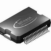
TLE6361G Infineon Technologies, TLE6361G Datasheet - Page 52

TLE6361G
Manufacturer Part Number
TLE6361G
Description
IC PS SYSTEM MULTI VOLT PDSO-36
Manufacturer
Infineon Technologies
Type
Step-Down (Buck)r
Datasheet
1.TLE6361G.pdf
(57 pages)
Specifications of TLE6361G
Internal Switch(s)
Yes
Synchronous Rectifier
No
Number Of Outputs
4
Voltage - Output
5.4 ~ 6.05 V
Current - Output
1.5A
Frequency - Switching
370kHz
Voltage - Input
5.5 ~ 60 V
Operating Temperature
-40°C ~ 150°C
Mounting Type
Surface Mount
Package / Case
DSO-36
Output Voltage
5.5 V
Output Current
1.5 A
Input Voltage Max
60 V
Maximum Operating Temperature
+ 150 C
Minimum Operating Temperature
- 40 C
Mounting Style
SMD/SMT
Operating Temperature Range
- 40 C to + 150 C
Output Voltage Tolerance
+/- 10 %
Lead Free Status / RoHS Status
Contains lead / RoHS non-compliant
Power - Output
-
Lead Free Status / Rohs Status
Lead free / RoHS Compliant
Other names
SP000013297
TLE6361GNT
TLE6361GT
TLE6361GNT
TLE6361GT
Available stocks
Company
Part Number
Manufacturer
Quantity
Price
Company:
Part Number:
TLE6361G
Manufacturer:
INFINEON
Quantity:
5 510
Part Number:
TLE6361G
Manufacturer:
INFINEON/英飞凌
Quantity:
20 000
5.2.5
The voltage at the Bootstrap capacitor does not exceed 15V, a ceramic type with a
minimum of 2% of the buck output capacitance and voltage class 16V would be
sufficient.
5.2.6
Out of the feedback voltage the charge pump generates a voltage between 8 and 10V.
The fly capacitor connected between C+ and C- is charged with the feedback voltage
level and discharged to achieve the (almost) double voltage level at CCP. C
to 100nF and C
The connection of CCP to a voltage source of e.g. 7V (take care of the maximum
ratings!) via a diode improves the start-up behavior at very low battery voltage. The diode
with the cathode on CCP has to be used in order to avoid any influence of the voltage
source to the device’s operation and vice versa.
5.2.7
At the input of Buck converters a square wave current is observed causing
electromagnetical interference on the battery line. The emission to the battery line
consists on one hand of components of the switching frequency (fundamental wave) and
its harmonics and on the other hand of the high frequency components derived from the
current slope. For proper attenuation of those interferers a -type input filter structure is
recommended which is built up with inductive (L
C
higher values might not be necessary, C
input capacitance with very low ESR should be chosen and placed as close to the input
of the Buck converter as possible.
Inexpensive input filters show due to their parasitrics a notch filter characteristic, which
means basically that the lowpass filter acts from a certain frequency as a highpass filter
and means further that the high frequency components are not attenuated properly. For
that reason the TLE 6361 G offers the possibility of current slope adjustment. The current
transistion time can be set by the external slew resistor to times between 20ns and 80ns
by varying the resistor value bewteen 0
transistion).
5.2.8
To decrease the switching losses to a mininum the external components R
and D
mA where the Diode D
If this feature is not needed the three components are not needed and the Boost pin (33)
can be connected directly to the IN pins(32, 30).
Data Sheet, Rev. 2.0
I3
). The inductance can be chosen up to the value of the Buck converter inductance,
Boost
Bootstrap capacitor (C
External charge pump capacitors (C
Input filter components for reduced EME (C
Feedback circuit for minimum switching loss (R
are needed. The current through the feedback resistor R
CCP
to 220nF, both ceramic types.
Boost
and the capacitor C
BTP
)
I1
and C
52
(fastest transition) and 20k
Boost
FLY
I3
I
) and capacitive components (C
should be ceramic types and for C
, C
run a part of the load current.
CCP
I1
)
, C
I2
Boost
, C
I3
, C
, L
Boost
I
, R
Boost
, D
Slew
is about a few
TLE 6361 G
Boost
)
FLY
Boost
2005-03-01
)
is chosen
(slowest
, C
I1
, C
I2
Boost
an
I2
,


