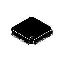
ADP3290JCPZ-RL ON Semiconductor, ADP3290JCPZ-RL Datasheet - Page 22

ADP3290JCPZ-RL
Manufacturer Part Number
ADP3290JCPZ-RL
Description
IC CTLR BUCK SW REG 40-LFCSP
Manufacturer
ON Semiconductor
Type
Step-Down (Buck)r
Datasheet
1.ADP3290JCPZ-RL.pdf
(30 pages)
Specifications of ADP3290JCPZ-RL
Internal Switch(s)
No
Synchronous Rectifier
Yes
Number Of Outputs
4
Voltage - Output
0.5 ~ 1.6 V
Frequency - Switching
250kHz ~ 4MHz
Voltage - Input
12V
Operating Temperature
0°C ~ 85°C
Mounting Type
Surface Mount
Package / Case
40-LFCSP
Output Voltage
0.5 V to 1.6 V
Output Current
500 uA
Input Voltage
- 0.3 V to + 6.3 V
Supply Current
25 mA
Switching Frequency
450 kHz
Mounting Style
SMD/SMT
Maximum Operating Temperature
+ 85 C
Minimum Operating Temperature
0 C
Lead Free Status / RoHS Status
Lead free / RoHS Compliant
Current - Output
-
Power - Output
-
Lead Free Status / Rohs Status
Lead free / RoHS Compliant
Available stocks
Company
Part Number
Manufacturer
Quantity
Price
5 mW each yields C
the bulk capacitors (L
frequency ringing during a load change.
This is tested using:
where Q
system.
Al−Poly capacitors, which satisfies this limitation. If the L
of the chosen bulk capacitor bank is too large, the number of
ceramic capacitors needs to be increased, or lower ESL
bulks need to be used if there is excessive undershoot during
a load transient.
designs can be used providing the conditions of Equation 19
through Equation 24 are satisfied.
Power MOSFETs
been selected for one high−side switch and two low−side
switches per phase. The main selection parameters for the
power MOSFETs are V
R
voltage to the ADP3120A dictates whether standard
threshold or logic−level threshold MOSFETs must be used.
With V
(V
requirement for the low−side (synchronous) MOSFETs.
With the ADP3290, currents are balanced between phases,
thus, the current in each low−side MOSFET is the output
DS(ON)
Using 8, 560 mF Al−Poly capacitors with a typical ESR of
One last check should be made to ensure that the ESL of
In this example, L
For this multi−mode control technique, all ceramic
For this example, the N−channel power MOSFETs have
The maximum output current (I
GS(TH)
where K = 5.39.
C
C
C
X(MIN)
X(MIN)
X(MAX)
. The minimum gate drive voltage (the supply
GATE
2
< 2.5 V) are recommended.
L
L
is limited to 4/3 to ensure a critically damped
X
Z
w
w
v
v C
v 396 mF
~10 V, logic−level threshold MOSFETs
4
n
4
Z
X
5.39
X
= 4.48 mF with an R
R
1.0 mW )
R
X
is approximately 250 pH for the 8,
220 nH
2
O
) is low enough to limit the high
O
2
L
220 nH
)
GS(TH)
1 mW
Q
D V
D I
1.0 mW
D I
2
O
rl
O
2
, Q
O
50 mV
95 A
1.1 V
) determines the R
95 A
G
4
3
2
V
, C
+ 528 pH
VID
1.4 V
ISS
X
* C
1.4 V
= 0.6 mW.
, C
Z
RSS
* 396 mF
(eq. 24)
DS(ON)
http://onsemi.com
, and
1 )
X
22
+ 2.08mF
233.75 ms
current divided by the total number of MOSFETs (n
With conduction losses being dominant, Equation 25 shows
the total power that is dissipated in each synchronous
MOSFET in terms of the ripple current per phase (I
average total output current (I
and the maximum allowed power dissipation, the user can
find the required R
MOSFETs up to an ambient temperature of 50°C, a safe
limit for P
Thus, for this example (115 A maximum), R
MOSFET) < 8.5 mW. This R
temperature of about 120°C. As a result, users need to
account for this when making this selection. This example
uses two lower−side MOSFETs at 10.5 mW, each at 120°C.
is the input capacitance and feedback capacitance. The ratio
of the feedback to input needs to be small (less than 10% is
recommended) to prevent accidental turn−on of the
synchronous MOSFETs when the switch node goes high.
should not exceed the non−overlap dead time of the
MOSFET driver (40 ns typical for the ADP3120A). The
output impedance of the driver is approximately 2 W, and the
typical MOSFET input gate resistances are about 1 W to 2 W.
Therefore, a total gate capacitance of less than 6000 pF
should be adhered to. Because two MOSFETs are in parallel,
the input capacitance for each synchronous MOSFET
should be limited to 3000 pF.
two main power dissipation components: conduction and
switching losses. The switching loss is related to the amount
P
SF
Knowing the maximum output current being designed for
Another important factor for the synchronous MOSFET
Also, the time to switch the synchronous MOSFETs off
The high−side (main) MOSFET has to be able to handle
+ ( 1 * D )
1.1 V
SF
1.4 V
is 1 W to 1.5 W at 120°C junction temperature.
220 nH
4
DS(ON)
n
I
5.39
SF
O
for the MOSFET. For D−PAK
2
) 1
O
* 396 mF + 41.5 mF
DS(SF)
1.0 mW
).
12
is also at a junction
n
nI
2
SF
R
* 1
2
DS(SF)
R
(eq. 25)
(eq. 21)
(eq. 22)
(eq. 23)
R
DS(SF)
) and
(per
SF
).


