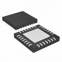
MAX1234ETI+T Maxim Integrated Products, MAX1234ETI+T Datasheet - Page 12

MAX1234ETI+T
Manufacturer Part Number
MAX1234ETI+T
Description
IC CNTRLR TOUCH 28-TQFN
Manufacturer
Maxim Integrated Products
Type
Resistiver
Datasheet
1.MAX1234ETIT.pdf
(44 pages)
Specifications of MAX1234ETI+T
Touch Panel Interface
4-Wire
Number Of Inputs/keys
1, 4 x 4 Keypad
Resolution (bits)
8, 10, 12 b
Data Interface
MICROWIRE™, QSPI™, Serial, SPI™
Data Rate/sampling Rate (sps, Bps)
50k
Voltage Reference
Internal
Voltage - Supply
4.75 V ~ 5.25 V
Operating Temperature
-40°C ~ 85°C
Mounting Type
Surface Mount
Package / Case
28-TQFN Exposed Pad
Applications
*
Lead Free Status / RoHS Status
Lead free / RoHS Compliant
±15kV ESD-Protected Touch-Screen
Controllers Include DAC and Keypad Controller
The MAX1233/MAX1234 are 4-wire touch-screen con-
trollers. Figure 1 shows the functional diagram of the
MAX1233/MAX1234. Each device includes a 12-bit sam-
pling ADC, 8-bit voltage output DAC, keypad scanner
that can also be configured as a GPIO, internal clock,
reference, temperature sensor, two battery monitor
inputs, two auxiliary analog inputs, SPI/QSPI/
MICROWIRE-compatible serial interface, and low on-
resistance switches for driving touch screens.
The 16-bit register inside the MAX1233/MAX1234
allows for easy control and stores results that can be
read at any time. The BUSY output indicates that a
functional operation is in progress. The PENIRQ and
KEYIRQ outputs, respectively, indicate that a screen
touch or a key press has occurred.
The 4-wire touch-screen controller works by creating a
voltage gradient across the vertical or horizontal resis-
tive touch screen connected to the analog inputs of the
MAX1233/MAX1234, as shown in Figure 2. The voltage
across the touch-screen panels is applied through inter-
nal MOSFET switches that connect each resistive layer
to AV
position when a pointing device presses on the touch
screen, the Y+ and Y- drivers are turned on, connecting
one side of the vertical resistive layer to AV
other side to ground. The horizontal resistive layer func-
tions as a sense line. One side of this resistive layer gets
connected to the X+ input, while the other side is left
* ESD protected: ±8kV Contact, ±15kV Air.
12
______________________________________________________________________________________
PIN
19
20
21
22
23
24
25
26
27
28
—
DD
and ground. For example, to measure the Y
PENIRQ
KEYIRQ
NAME
DOUT
BUSY
SCLK
DIN
C2
C3
C4
CS
EP
Detailed Description
Touch-Screen Operation
Keypad Column 2. Can be reconfigured as GPIO5.
Keypad Column 3. Can be reconfigured as GPIO6.
Keypad Column 4. Can be reconfigured as GPIO7.
Active-Low Keypad Interrupt. KEYIRQ is low when a key press is detected.
Active-Low Pen Touch Interrupt. PENIRQ is low when a screen touch is detected.
Serial Data Output. Data is clocked out at SCLK falling edge. High impedance when CS is high.
Active-Low Busy Output. BUSY goes low and stays low during each functional operation. The host
controller should wait until BUSY is high again before using the serial interface.
Serial Data Input. Data is clocked in on the rising edge of SCLK.
Serial Clock Input. Clocks data in and out of the serial interface and sets the conversion speed (duty
cycle must be 30% to 70%).
Active-Low Chip Select. Data is not clocked into DIN unless CS is low. When CS is high, DOUT is
high impedance.
Exposed Pad. Internally connected to GND. Connect to a large ground plane to maximize thermal
performance. Not intended as an electrical connection point.
DD
and the
open or floating. The point where the touch screen is
pressed brings the two resistive layers in contact and
creates a voltage-divider at that point. The data convert-
er senses the voltage at the point of contact through the
X+ input and digitizes it.
Figure 3 shows a block diagram of the ADC’s analog
input section including the input multiplexer, the differen-
tial input, and the differential reference. The input multi-
plexer switches between X+, X-, Y+, Y-, AUX1, AUX2,
BAT1, BAT2, and the internal temperature sensor.
The time required for the T/H to acquire an input signal
is a function of how quickly its input capacitance is
charged. If the input signal’s source impedance is high,
the acquisition time lengthens, and more time must be
allowed. The acquisition time (t
time the device takes to acquire the input signal to 12-
bit accuracy. Configure t
control register. See Table 1 for the maximum input sig-
nal source impedance (R
during acquisition.
Accommodate higher source impedances by placing a
0.1µF capacitor between the analog input and GND.
The ADC’s input-tracking circuitry has a 0.5MHz small-
signal bandwidth. To avoid high-frequency signals
being aliased into the frequency band of interest, anti-
alias filtering is recommended.
FUNCTION
Pin Description (continued)
SOURCE
ACQ
by writing to the ADC
ACQ
) for complete settling
) is the maximum
Input Bandwidth
Analog Inputs
12-Bit ADC


