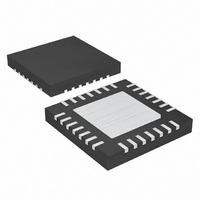
MAX1234ETI+T Maxim Integrated Products, MAX1234ETI+T Datasheet - Page 26

MAX1234ETI+T
Manufacturer Part Number
MAX1234ETI+T
Description
IC CNTRLR TOUCH 28-TQFN
Manufacturer
Maxim Integrated Products
Type
Resistiver
Datasheet
1.MAX1234ETIT.pdf
(44 pages)
Specifications of MAX1234ETI+T
Touch Panel Interface
4-Wire
Number Of Inputs/keys
1, 4 x 4 Keypad
Resolution (bits)
8, 10, 12 b
Data Interface
MICROWIRE™, QSPI™, Serial, SPI™
Data Rate/sampling Rate (sps, Bps)
50k
Voltage Reference
Internal
Voltage - Supply
4.75 V ~ 5.25 V
Operating Temperature
-40°C ~ 85°C
Mounting Type
Surface Mount
Package / Case
28-TQFN Exposed Pad
Applications
*
Lead Free Status / RoHS Status
Lead free / RoHS Compliant
±15kV ESD-Protected Touch-Screen
Controllers Include DAC and Keypad Controller
The data results from conversions or keypad scans are
held in the data registers of the MAX1233/MAX1234.
During power-up, all of these data registers with the
exception of the DAC data register default to 0000
The DAC register defaults to 1000
Table 25. Keypad Column Mask Register Bit Descriptions (Write 0x0051/Read 0x8051)
Table 26. GPIO Control Register (Write 0x004F/Read 0x804F)
Table 27. GPIO Control Register Bit Descriptions (Write 0x004F/Read 0x804F)
Table 28.GPIO Pullup Disable Register (Write 0x004E/Read 0x804E)
Table 29. GPIO Pullup Disable Register
Descriptions
26
BIT15 BIT14 BIT13 BIT12 BIT11 BIT10
BIT15 BIT14 BIT13 BIT12 BIT11 BIT10
[15:8]
GP7
PU7
[7:0]
BIT
[11:0]
[7:0]
______________________________________________________________________________________
BIT
BIT
15
14
13
12
15
14
13
12
11
10
9
8
GP6
PU6
[PU7:PU0]
NAME
0
[OE7:OE0]
GP5
PU5
NAME
NAME
CM4
CM3
CM2
CM1
GP7
GP6
GP5
GP4
GP3
GP2
GP1
GP0
0
1: P ul l up d i sab l ed . Op en col l ector outp ut.
0: Pullup enabled.
Reserved: always write as zero.
GP4
PU4
Mask interrupt, status register, and pending register data update on all keys in column 4
Mask interrupt, status register, and pending register data update on all keys in column 3
Mask interrupt, status register, and pending register data update on all keys in column 2
Mask interrupt, status register, and pending register data update on all keys in column 1
Reserved
GPIO pin configured as an output
C4 pin becomes GPIO pin 7
C3 pin becomes GPIO pin 6
C2 pin becomes GPIO pin 5
C1 pin becomes GPIO pin 4
R4 pin becomes GPIO pin 3
R3 pin becomes GPIO pin 2
R2 pin becomes GPIO pin 1
R1 pin becomes GPIO pin 0
GP3
PU3
DESCRIPTION
H
.
GP2
PU2
Data Registers
BIT9
BIT9
GP1
PU1
1
BIT8
BIT8
GP0
PU0
H
.
BIT7
BIT7
OE7
Table 30 shows the format of the X, Y, Z
BAT2, AUX1, AUX2, TEMP1, and TEMP2 data registers.
The data format for these registers is right justified
beginning with bit 11. Data written through the serial
interface to these registers is not stored.
Table 31 shows the formatting of the keypad data regis-
ters, while Tables 32, 33, and 34 provide individual reg-
ister bit descriptions. These registers have the same
format as the keypad mask register. Each bit repre-
sents one key on the keypad. Table 35 shows a map of
a 16-key keypad. Data written through the serial inter-
face to these registers is not stored.
0
DESCRIPTION
DESCRIPTION
BIT6
BIT6
OE6
0
C4 pin remains keypad column 4
C3 pin remains keypad column 3
C2 pin remains keypad column 2
C1 pin remains keypad column 1
R4 pin remains keypad row 4
R3 pin remains keypad row 3
R2 pin remains keypad row 2
R1 pin remains keypad row 1
GPIO pin configured as an input
BIT5
BIT5
OE5
0
BIT4
BIT4
OE4
0
Analog Input Data Registers
BIT3
BIT3
OE3
0
Keypad Data Registers
0
BIT2
BIT2
OE2
0
BIT1
1
BIT1
OE1
, Z
0
2
, BAT1,
BIT0
BIT0
OE0
0


