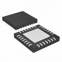
MAX1234ETI+T Maxim Integrated Products, MAX1234ETI+T Datasheet - Page 23

MAX1234ETI+T
Manufacturer Part Number
MAX1234ETI+T
Description
IC CNTRLR TOUCH 28-TQFN
Manufacturer
Maxim Integrated Products
Type
Resistiver
Datasheet
1.MAX1234ETIT.pdf
(44 pages)
Specifications of MAX1234ETI+T
Touch Panel Interface
4-Wire
Number Of Inputs/keys
1, 4 x 4 Keypad
Resolution (bits)
8, 10, 12 b
Data Interface
MICROWIRE™, QSPI™, Serial, SPI™
Data Rate/sampling Rate (sps, Bps)
50k
Voltage Reference
Internal
Voltage - Supply
4.75 V ~ 5.25 V
Operating Temperature
-40°C ~ 85°C
Mounting Type
Surface Mount
Package / Case
28-TQFN Exposed Pad
Applications
*
Lead Free Status / RoHS Status
Lead free / RoHS Compliant
These bits specify the time delay from pen-touch detec-
tion to a conversion start. This allows the selection of the
appropriate settling time for the touch screen being used.
Table 11 shows how to set the settling time. These bits
are identical, regardless of read or write.
This bit selects the ADC internal reference voltage,
either +1.0V or +2.5V. This bit is identical, regardless of
read or write. The reference control bit is shown in
Table 12.
Table 11. Touch-Screen Settling Time
Control*
* Applicable only for X, Y, Z1, and Z2 measurements.
Table 12. ADC Reference Control Bit
Table 13. Internal ADC Reference Auto Power-Up Control
Table 14. DAC Control Register (Write 0x0042/Read 0x8042)
BIT15 BIT14 BIT13 BIT12 BIT11 BIT10
DAPD
[A/D3:A/D0]
Controllers Include DAC and Keypad Controller
ST2
0
0
0
0
1
1
1
1
0000
0000
0000
0000
Bit 0: ADC Internal Reference Voltage Control
Bits 1-3: Touch-Screen Settling Time Control
RFV
0
1
0
ST1
0
0
1
1
0
0
1
1
RES1
0
______________________________________________________________________________________
ST0
0
0
1
1
0
1
0
1
0
1
0
1
0
Settling time: 0µs
Settling time: 100µs
Settling time: 500µs
Settling time: 1ms
Settling time: 5ms
Settling time: 10ms
Settling time: 50ms
Settling time: 100ms
±15kV ESD-Protected Touch-Screen
RES0
+1.0V reference
+2.5V reference
0
1
0
1
0
SETTLING TIME
FUNCTION
A DC R EF ER EN C E
0
SOURCE
External
External
Internal
Internal
BIT9
0
BIT8
0
Power up, wait for reference to settle, and power down again for
each temperature, battery, or auxiliary scan (auto power-up mode)
Always powered up
Always powered down
Always powered down
BIT7
The ADC control register controls the power setting of
the internal ADC reference. Zeros must be written to
bits A/D3–A/D0 to control internal reference power-up
followed by the appropriate logic at the RES1 and RES0
bits. Table 13 shows the internal ADC reference power-
down control.
The MSB in this control register determines the power-
down control of the on-board DAC. Table 14 shows the
DAC control register. Writing a zero to bit 15 (DAPD)
powers up the DAC, while writing a 1 powers down the
DAC. Table 15 describes the DAC control register con-
tents, while Table 16 shows the DAC power-down bit.
The keypad control register, keypad mask register, and
keypad column mask control register control the key-
pad scanner in the MAX1233/MAX1234. The keypad
control register (Table 17) controls scanning and
debouncing, while the keypad mask register (Table 22)
and the keypad column mask control register (Table 24),
Table 15. DAC Control Register
Descriptions
Table 16. DAC Power-Down Bit
0
15 (MSB)
[14:0]
BIT
BIT6
DAPC
Internal ADC Reference Power-Down Control
0
0
1
ADC REFERENCE POWER MODE
NAME
DAPD
BIT5
0
0
BIT4
0
Keypad Control Registers
BIT3
DAC powered down
DAC powered down
0
DAC powered up
DESCRIPTION
DAC Control Register
FUNCTION
Reserved
BIT2
0
BIT1
0
BIT0
0
23


