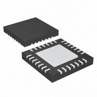
MAX1234ETI+T Maxim Integrated Products, MAX1234ETI+T Datasheet - Page 2

MAX1234ETI+T
Manufacturer Part Number
MAX1234ETI+T
Description
IC CNTRLR TOUCH 28-TQFN
Manufacturer
Maxim Integrated Products
Type
Resistiver
Datasheet
1.MAX1234ETIT.pdf
(44 pages)
Specifications of MAX1234ETI+T
Touch Panel Interface
4-Wire
Number Of Inputs/keys
1, 4 x 4 Keypad
Resolution (bits)
8, 10, 12 b
Data Interface
MICROWIRE™, QSPI™, Serial, SPI™
Data Rate/sampling Rate (sps, Bps)
50k
Voltage Reference
Internal
Voltage - Supply
4.75 V ~ 5.25 V
Operating Temperature
-40°C ~ 85°C
Mounting Type
Surface Mount
Package / Case
28-TQFN Exposed Pad
Applications
*
Lead Free Status / RoHS Status
Lead free / RoHS Compliant
±15kV ESD-Protected Touch-Screen
Controllers Include DAC and Keypad Controller
ABSOLUTE MAXIMUM RATINGS
AV
DV
Digital Inputs/Outputs to GND .................-0.3V to (DV
X+, Y+, X-, Y-, AUX1, AUX2,
BAT1, BAT2 to GND .................................................-0.3V to +6V
Maximum ESD per IEC 1000-4-2 (per MIL STD-883 HBM)
ELECTRICAL CHARACTERISTICS
(DV
(MAX1233), V
+85°C, unless otherwise noted. Typical values are at T
Stresses beyond those listed under “Absolute Maximum Ratings” may cause permanent damage to the device. These are stress ratings only, and functional
operation of the device at these or any other conditions beyond those indicated in the operational sections of the specifications is not implied. Exposure to
absolute maximum rating conditions for extended periods may affect device reliability.
2
DC ACCURACY (Note 1)
Resolution
No Missing Codes
Relative Accuracy (Note 2)
Differential Nonlinearity
Offset Error
Gain Error (Note 3)
Total Unadjusted Error
Offset Temperature Coefficient
Gain Temperature Coefficient
Channel-to-Channel Offset
Channel-to-Channel Gain
Matching
Noise
Power-Supply Rejection
DYNAMIC SPECIFICATIONS (1kHz SINE WAVE, V
f
Signal-to-Noise Plus Distortion
SCLK
and REF to GND ..................................-0.3V to (AV
X+, X-, Y+, Y-, AUX1, AUX2, BAT1, BAT2......................±15kV
DD
DD
DD
_______________________________________________________________________________________
to GND............................................................-0.3V to +6V
to AV
= AV
= 10MHz)
PARAMETER
DD
DD
REF
.......................................................-0.3V to +0.3V
= +2.7V to +3.6V (MAX1233), DV
= 4.096V (MAX1234); f
SYMBOL
SINAD
DNL
TUE
PSR
INL
SCLK
ANALOG-TO-DIGITAL CONVERTER
= 10MHz, f
Software-programmable 8/10/12 bit
12-bit mode
10-bit and 8-bit modes
12-bit mode
10-bit and 8-bit modes
12-bit mode
10-bit and 8-bit modes
12-bit mode
10-bit mode
8-bit mode
12-bit mode
10-bit and 8-bit modes
Including internal V
Full-scale
input
DD
DD
DD
IN
A
= 2.5V
+ 0.3V)
+ 0.3V)
= AV
= +25°C.)
SAMPLE
DD
MAX1233
AV
MAX1234
AV
P-P
CONDITIONS
DD
DD
= +4.75V to +5.25V (MAX1234), external reference V
FOR MAX1233, V
= DV
= DV
= 50ksps, 12-bit mode, 0.1µF capacitor at REF, T
REF
All Other Pins.....................................................................±2.5kV
Maximum Current into Any Pin............................................50mA
Continuous Power Dissipation (T
Operating Temperature Range ...........................-40°C to +85°C
Storage Temperature Range .............................-60°C to +150°C
Lead Temperature (soldering, 10s) .................................+300°C
28-Pin QFN (derate 28.5mW/°C above +70°C) .................2W
28-Pin TQFN (derate 28.5mW/°C above +70°C) ...............2W
DD
DD
= +2.7V to +3.6V
= +5V ±5%
IN
= 4.096V
P-P
MIN
11
FOR MAX1234, 50ksps,
A
= +70°C)
TYP
±0.8
±0.5
±0.8
±0.5
±0.5
±0.5
±0.5
±0.5
±0.5
±0.4
±0.4
±0.1
±0.1
±0.4
±0.3
±2
±1
50
69
MAX
12
±2
±2
±4
±4
A
REF
= -40°C to
ppm/°C
ppm/°C
UNITS
µV
= 2.5V
LSB
LSB
LSB
LSB
LSB
LSB
LSB
Bits
Bits
mV
dB
RMS


