AD9516-1/PCBZ Analog Devices Inc, AD9516-1/PCBZ Datasheet - Page 10
AD9516-1/PCBZ
Manufacturer Part Number
AD9516-1/PCBZ
Description
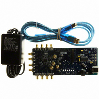
BOARD EVALUATION FOR AD9516-1
Manufacturer
Analog Devices Inc
Specifications of AD9516-1/PCBZ
Main Purpose
Timing, Clock Generator
Embedded
No
Utilized Ic / Part
AD9516-1
Primary Attributes
2 Inputs, 14 Outputs, 2.5GHz VCO
Secondary Attributes
CMOS, LVDS, LVPECL Output Logic, ADIsimCLK™ Graphical User Interface
Silicon Manufacturer
Analog Devices
Application Sub Type
PLL Clock Synthesizer
Kit Application Type
Clock & Timing
Silicon Core Number
AD9516-0, AD9516-1, AD9516-2
Silicon Family Name
AD9516-X
Rohs Compliant
Yes
Lead Free Status / RoHS Status
Lead free / RoHS Compliant


UG-075
The evaluation software has internal checking to ensure that
invalid settings are not programmed. For example, the B
counter must always be larger than the A counter. Another
restriction is that 8/9 dual modulus mode cannot be used for
VCO frequencies greater than 2400 MHz. In cases where a
feedback divider restriction cannot be resolved, you may need
to adjust the R (reference) divider to allow a different feedback
divider value. For example, it is not possible to use the internal
VCO, and a feedback divider of 30. However, the R divider can
be doubled, which allows a feedback divider of 60.
The feedback divider window has a check box for holding the
N divider in reset. When the N divider is held in reset, the PLL
loop is open. Therefore, this feature is seldom used.
PHASE FREQUENCY DETECTOR (PFD) WINDOW
The Phase Frequency Detector (PFD) window shown in
Figure 15 is accessed by clicking the PFD box on the main
window.
The features accessible in this window are described in detail in
the AD951x data sheet. The most commonly used settings are
the Anti-Backlash Pulse Width and the Lock Detect Counter.
For phase detector frequencies greater than 50 MHz, the PLL
may work better with the 1.3 ns antibacklash pulse width setting.
Setting the lock detect counter to values greater then 5 PFD
cycles can be useful in applications where the loop bandwidth
is low and the lock detect counter chatters during acquisition.
Figure 15. Phase Frequency Detector Window
Rev. 0 | Page 10 of 16
CHARGE PUMP WINDOW
The Charge Pump Setup window shown in Figure 16 is accessed
by clicking the CHARGE PUMP box on the main screen.
This window is most often used to vary the charge pump
current.
The window also has a check box for setting the charge pump
voltage to V
isolating the output driver section of the AD951x from the PLL
section.
VCO CALIBRATION WINDOW
The Calibrate VCO window shown in Figure 17 is accessed by
clicking the Cal VCO button on the main window.
A valid reference input signal must be present to complete VCO
calibration, and the VCO must be recalibrated any time the
VCO frequency changes by more than 40 MHz.
A VCO divider of 16 is suitable for all applications. However,
for applications where the phase detector frequency is <12 MHz,
using a smaller VCO calibration divider reduces calibration
time. Refer to the AD951x data sheet for more details.
Note that the automatic holdover feature must not be enabled
during VCO calibration. See the PLL Configuration Window
section, and make sure that the Enable Hold Over check box
is cleared during VCO calibration.
CP
/2, which is very useful for debugging the PLL and
Figure 16. Charge Pump Setup Window
Evaluation Board User Guide
Figure 17. Calibrate VCO Window
Related parts for AD9516-1/PCBZ
Image
Part Number
Description
Manufacturer
Datasheet
Request
R

Part Number:
Description:
IC CLOCK PLL/VCO 2GHZ 64LFCSP
Manufacturer:
Analog Devices Inc
Datasheet:
Part Number:
Description:
IC CLOCK GEN 2.8GHZ VCO 64-LFCSP
Manufacturer:
Analog Devices Inc
Datasheet:
Part Number:
Description:
IC,Fourteen Distributed-Output Clock Driver,LLCC,64PIN,PLASTIC
Manufacturer:
Analog Devices Inc
Datasheet:
Part Number:
Description:
IC,Ten Distributed-Output Clock Driver,LLCC,64PIN,PLASTIC
Manufacturer:
Analog Devices Inc
Datasheet:
Part Number:
Description:
IC,Ten Distributed-Output Clock Driver,LLCC,64PIN,PLASTIC
Manufacturer:
Analog Devices Inc
Datasheet:
Part Number:
Description:
Clock IC With 1.8GHz On-chip VCO
Manufacturer:
Analog Devices Inc
Datasheet:

Part Number:
Description:
BOARD EVAL FOR AD9516-3 2.0GHZ
Manufacturer:
Analog Devices Inc
Datasheet:

Part Number:
Description:
BOARD EVAL FOR AD9516-4 1.8GHZ
Manufacturer:
Analog Devices Inc
Datasheet:
Part Number:
Description:
IC,Ten Distributed-Output Clock Driver,LLCC,64PIN,PLASTIC
Manufacturer:
Analog Devices Inc
Datasheet:
Part Number:
Description:
IC,Fourteen Distributed-Output Clock Driver,LLCC,64PIN,PLASTIC
Manufacturer:
Analog Devices Inc
Datasheet:
Part Number:
Description:
IC,Ten Distributed-Output Clock Driver,LLCC,64PIN,PLASTIC
Manufacturer:
Analog Devices Inc
Datasheet:
Part Number:
Description:
Clock IC With 1.8GHz On-chip VCO
Manufacturer:
Analog Devices Inc
Datasheet:
Part Number:
Description:
10/14 Chan Clock IC W/PLL-no VCO
Manufacturer:
Analog Devices Inc
Datasheet:
Part Number:
Description:
10/14 Chan Clock IC W/PLL-no VCO
Manufacturer:
Analog Devices Inc
Datasheet:

Part Number:
Description:
Clock IC With 2.5GHz On-chip VCO EB
Manufacturer:
Analog Devices Inc
Datasheet: