AD9516-1/PCBZ Analog Devices Inc, AD9516-1/PCBZ Datasheet - Page 5
AD9516-1/PCBZ
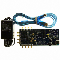
Manufacturer Part Number
AD9516-1/PCBZ
Description
BOARD EVALUATION FOR AD9516-1
Manufacturer
Analog Devices Inc
Specifications of AD9516-1/PCBZ
Main Purpose
Timing, Clock Generator
Embedded
No
Utilized Ic / Part
AD9516-1
Primary Attributes
2 Inputs, 14 Outputs, 2.5GHz VCO
Secondary Attributes
CMOS, LVDS, LVPECL Output Logic, ADIsimCLK™ Graphical User Interface
Silicon Manufacturer
Analog Devices
Application Sub Type
PLL Clock Synthesizer
Kit Application Type
Clock & Timing
Silicon Core Number
AD9516-0, AD9516-1, AD9516-2
Silicon Family Name
AD9516-X
Rohs Compliant
Yes
Lead Free Status / RoHS Status
Lead free / RoHS Compliant


Evaluation Board User Guide
QUICK START GUIDE TO THE AD9516 PLL
When the evaluation software is installed, the evaluation board
is connected, and the software is loaded, use the following steps
to configure and lock the PLL. These steps assume that the input
signal is present, the evaluation board has not been modified,
and that the PLL loop filter is suitable for the user’s application.
This quick start guide covers only simple PLL operation to
start the PLL. See the AD9516 data sheet and Evaluation
Software Components section for a detailed explanation
of the various AD9516 features.
The following case is an example for the AD9516-3 using the
values in Table 1.
Table 1.
Parameter
Input Frequency
Output Frequency
Reference Divider
Phase Detector Frequency
Feedback Divider
VCO Frequency
VCO Divider
Channel Divider
1.
2.
3.
Turn the PLL on by selecting Normal Op from the PLL
MODE box found at the top of the main window (see
Figure 8).
Enter the intended reference input frequency (in
megahertz) in the REF 1 (MHz) box at the upper left
corner of the main window.
Click the triangular buffer symbol immediately to the right
of the input reference frequency (see Figure 4) boxes to load
the Reference Input Control window shown in Figure 5.
Turn the REF1 reference input buffer on by selecting the
Enable REF1 check box, and then clicking OK.
Figure 4. Buffer Symbol
Value
20 MHz on REF1
200 MHz on OUT1
2
10 MHz
200
2000 MHz
2
5
Rev. 0 | Page 5 of 16
4.
5.
When the window closes, the WRITE button under the
REGISTER W/R section in the main window blinks red.
This indicates there are settings that have not been loaded
to the AD9516 evaluation board. Click the blinking red
WRITE button to load these settings to the evaluation
board.
Select the VCO as the input to the clock distribution
circuitry by clicking the mux symbol that is located
immediately to the right of the VCO (MHz) box (see
Figure 6).
When the VCO is selected, the border of the VCO (MHz)
box changes from gray to black. The current VCO
frequency is shown in the VCO (MHz) box.
Figure 5. Reference Input Control Window
Figure 6. Buffer Symbol
UG-075
Related parts for AD9516-1/PCBZ
Image
Part Number
Description
Manufacturer
Datasheet
Request
R

Part Number:
Description:
IC CLOCK PLL/VCO 2GHZ 64LFCSP
Manufacturer:
Analog Devices Inc
Datasheet:
Part Number:
Description:
IC CLOCK GEN 2.8GHZ VCO 64-LFCSP
Manufacturer:
Analog Devices Inc
Datasheet:
Part Number:
Description:
IC,Fourteen Distributed-Output Clock Driver,LLCC,64PIN,PLASTIC
Manufacturer:
Analog Devices Inc
Datasheet:
Part Number:
Description:
IC,Ten Distributed-Output Clock Driver,LLCC,64PIN,PLASTIC
Manufacturer:
Analog Devices Inc
Datasheet:
Part Number:
Description:
IC,Ten Distributed-Output Clock Driver,LLCC,64PIN,PLASTIC
Manufacturer:
Analog Devices Inc
Datasheet:
Part Number:
Description:
Clock IC With 1.8GHz On-chip VCO
Manufacturer:
Analog Devices Inc
Datasheet:

Part Number:
Description:
BOARD EVAL FOR AD9516-3 2.0GHZ
Manufacturer:
Analog Devices Inc
Datasheet:

Part Number:
Description:
BOARD EVAL FOR AD9516-4 1.8GHZ
Manufacturer:
Analog Devices Inc
Datasheet:
Part Number:
Description:
IC,Ten Distributed-Output Clock Driver,LLCC,64PIN,PLASTIC
Manufacturer:
Analog Devices Inc
Datasheet:
Part Number:
Description:
IC,Fourteen Distributed-Output Clock Driver,LLCC,64PIN,PLASTIC
Manufacturer:
Analog Devices Inc
Datasheet:
Part Number:
Description:
IC,Ten Distributed-Output Clock Driver,LLCC,64PIN,PLASTIC
Manufacturer:
Analog Devices Inc
Datasheet:
Part Number:
Description:
Clock IC With 1.8GHz On-chip VCO
Manufacturer:
Analog Devices Inc
Datasheet:
Part Number:
Description:
10/14 Chan Clock IC W/PLL-no VCO
Manufacturer:
Analog Devices Inc
Datasheet:
Part Number:
Description:
10/14 Chan Clock IC W/PLL-no VCO
Manufacturer:
Analog Devices Inc
Datasheet:

Part Number:
Description:
Clock IC With 2.5GHz On-chip VCO EB
Manufacturer:
Analog Devices Inc
Datasheet: