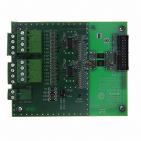
STEVAL-IFP007V1 STMicroelectronics, STEVAL-IFP007V1 Datasheet
STEVAL-IFP007V1
Specifications of STEVAL-IFP007V1


Related parts for STEVAL-IFP007V1


STEVAL-IFP007V1 Summary of contents
Page 1
Protected digital input termination with serialized state transfer Features ■ 8-input circuit in common ground low side topology ■ Wide range input DC voltage V – On state threshold : < with R – Off state threshold: I ...
Page 2
Contents Contents 1 Circuit block diagram . . . . . . . . . . . . . . . . . . . . . . . . . . . . . . . . . . ...
Page 3
SCLT3-8BT8 3.5.2 3.6 Under voltage alarm setting for IEC and device-net applications . . . . . . . 27 3.7 Input operation for the device-net applications . . . . . . . . . . . . . ...
Page 4
Circuit block diagram 1 Circuit block diagram Figure 1. Circuit block diagram COM COM COM ...
Page 5
SCLT3-8BT8 1.1 I/O pin descriptions Table 1. I/O pin descriptions Name Type IN Power input I LD Power output I V Power input C V Signal input CS COM Ground P V Power output 5 V logic power supply DD ...
Page 6
Circuit block diagram Figure 3. Basic application diagram REF REF REF REF REF ...
Page 7
SCLT3-8BT8 2 Functional description 2.1 Input power section The SCLT3 8-line input termination device designed for automation applications. It provides the front-end circuitry of a digital input module (I/O) in industrial automation. Available in an ...
Page 8
Functional description Figure 5. Low side front-end input topology including the ESD surge protection and the LED driver 2.3 The input digital filter A digital filter is implemented between the input state comparator and the input state register. It consists ...
Page 9
SCLT3-8BT8 Figure 6. Two-step digital filter placed after the analog section of the logic input CKF CKF 2.4 Operation of the SCLT with the SPI bus The SPI bus master controller manages the data transfer with the chip select signal ...
Page 10
Functional description 2.5 SPI bus signal description 2.5.1 Chip select /CS When the chip select signal /CS is high, the data transfer is disabled (SCK and MOSI signals are ignored) and the data output MISO is in high impedance tri-state ...
Page 11
SCLT3-8BT8 2.5.5 SPI shift register operation selector SPM The input SPM allows the operation of the SPI shift register to be configured for an 8-bit or 16-bit operation. When SPM is set low (COM input state bits and the control ...
Page 12
Functional description 2.6.3 SPI transfer speed The speed of the SPI is defined by the clock frequency and the data frame transfer time. In the SCLT application the transfer time correspond to the input scanning time programmed by the I/O ...
Page 13
SCLT3-8BT8 Figure 10. SPI shift register data transfer sequence versus SCLT input states /CS=”1” /CS=”1” /CS /CS SCK1 SCK1 SCK1 SCK1 SCK2 SCK2 SCK15 SCK15 SCK16 SCK16 SCK16 SCK16 /CS /CS SCK1 SCK1 2.7 Control bit signals of the SPI ...
Page 14
Functional description Figure 11. UVA circuit block diagram The power supply diagnostics help to determine if the input state is really low or if some power bus failure is damaging the quality of this state signal. 2.7.2 Over temperature alarm ...
Page 15
SCLT3-8BT8 It is supposed such disturbances affect one bit at a time during the SPI frame transfer. EFT burst repetition rate is about 200 µs (5 kHz) and the SPI 16-bit frame should last less than 160 µs. A parity ...
Page 16
Functional description Table 5. Logic state of the SPI output versus the power loss signal POR and the SPI chip select /CS POR / Figure 13. Logic status of the ...
Page 17
SCLT3-8BT8 Table 6. Absolute ratings Symbol Pin MISO ...
Page 18
Functional description Table 8. Operating conditions Symbol Pin REF REF R OSC osc F IN ...
Page 19
SCLT3-8BT8 Table 9. DC electrical characteristics Symbol Pin Name I IN Input limiting current LIM V IN Low current input voltage LOW Current limiter activation V IN LIM TH voltage V IN, V Clamping voltage ...
Page 20
Functional description Table 9. DC electrical characteristics Symbol Pin Name V V Power voltage alarm CON CC ΔV OFF - V Voltage release hysteresis Input activation voltage Input hysteresis voltage HY CS ...
Page 21
SCLT3-8BT8 Table 10. SPI serial bus link electrical characteristics Symbol Pin Name t SCK Enable lead time LD t SCK Clock hold time HC t /CS Transfer delay time DT C Input capacitance IN SCK, t /CS, Input filter time ...
Page 22
Functional description Table 11. Electromagnetic compatibility ratings Symbol Node V V PPB ESD V V ESD ° 2.2 kΩ unless otherwise specified. ...
Page 23
SCLT3-8BT8 Figure 15. Typical limiting current I Figure 16. Relative variation of minimum filter time T temperature T versus junction temperature T LIM I (mA) LIM 2.8 Ω R ref = 15 k with 2 ...
Page 24
Application considerations 3 Application considerations 3.1 SCLT serial link configurations As long as /CS is low, a slave is able to transmit data bits whatever the length of the data frames. This feature allows several SCLT circuits to be connected ...
Page 25
SCLT3-8BT8 3.1.1 Interfacing the SPI section to the I/O controller through optotransistors Figure 18. Opto-couplers connection between dual SCLT circuit and their master bus controller 5V.REG 5V.REG V DD1 SCLT3 - 8 SPI data output 3.2 High speed operation with ...
Page 26
Application considerations 3.3 Reverse polarity robustness Any reverse polarity of an input IN not disturb the operation of the other input channels as long as the power supply is working properly (V >19 V). CC Such a case is not ...
Page 27
... The power supply resistor R current consumption. The V diode D to fit the 1 kV surge requirement. In this case SMAJ30A Transil™ diode are indicated. TM Transil is a trademark of STMicroelectronics can be added to meet mainly the IEC 61000-4-6 conducted RFI immunity. I and monitored by the UVA block through the input resistance ...
Page 28
Application considerations Figure 21. Power supply connection versus IEC 61131-2 norm levels (left) and device-net norm levels (right 3.7 Input operation for the device-net applications If ...
Page 29
SCLT3-8BT8 4 Ordering information scheme Figure 23. Ordering information scheme SCLT = Serial output current limiting termination current setting 8 = Eight channels B = EMC Level ± HTSSOP-38 package according to IEC ...
Page 30
Package information 5 Package information ● Epoxy meets UL94, V0 ● Lead-free packages In order to meet environmental requirements, ST offers these devices in different grades of ® ECOPACK packages, depending on their level of environmental compliance. ECOPACK specifications, grade ...
Page 31
SCLT3-8BT8 Figure 24. SCLT3-8BT8 footprint (dimensions in mm) 0.5 0.60 7.10 4.50 6.60 0.3 Doc ID 15191 Rev 3 Package information 1.30 3.30 31/33 ...
Page 32
Ordering information 6 Ordering information Table 14. Ordering information Order code SCLT3-8BT8-TR SCLT3-8BT8 7 Revision history Table 15. Document revision history Date 17-Nov-2008 04-May-2009 02-Nov-2009 32/33 Marking Package SCLT3-8BT8 HTSSOP-38 SCLT3-8BT8 HTSSOP-38 Revision 1 Initial release. 2 Updated mechanical data ...
Page 33
... SCLT3-8BT8 Information in this document is provided solely in connection with ST products. STMicroelectronics NV and its subsidiaries (“ST”) reserve the right to make changes, corrections, modifications or improvements, to this document, and the products and services described herein at any time, without notice. All ST products are sold pursuant to ST’s terms and conditions of sale. ...