STEVAL-IFP007V1 STMicroelectronics, STEVAL-IFP007V1 Datasheet - Page 27
STEVAL-IFP007V1
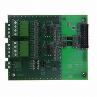
Manufacturer Part Number
STEVAL-IFP007V1
Description
BOARD EVAL BASED ON SCLT3-8
Manufacturer
STMicroelectronics
Specifications of STEVAL-IFP007V1
Main Purpose
Interface, Digital Signal Termination
Embedded
No
Utilized Ic / Part
SCLT3-8
Primary Attributes
8 Channel Optical Isolation
Secondary Attributes
SPI Interface
Processor To Be Evaluated
SCLT3
Data Bus Width
16 bit
Interface Type
SPI
Operating Supply Voltage
24 V
Lead Free Status / RoHS Status
Lead free / RoHS Compliant
Other names
497-9045


SCLT3-8BT8
3.5
3.5.1
3.5.2
3.6
Fast transient burst immunity
Considerations on the power section
The EFT protection is achieved with the same strategy as ESD and surge protection. An
input capacitor C
These capacitors play a key role in suppressing front-end electrical stresses. Their
capacitance can be about 22 nF (to validate by test for both EFT and RFI tests).
Detailed considerations for EMC performances, board design precautions and component
selections are also described in ST application notes AN2846 and AN2853.
Considerations on the logic section
The SPI section is not submitted directly to the transient burst disturbance because this
disturbance is applied to the logic input wires and the power supply wires.
Since the power section is protected with the clamping diodes, their serial impedance and
the digital filters, the logic section and the serial interface is protected against the effects of
transients.
Nevertheless, the SPI section may be submitted to indirect effects of the EFT transients. So,
the design of the power supplies (V
board are done with care to minimize the layout influences.
As shown on the suggested opto-transistor schematic on
power supply decoupling capacitors should be added to meet the reinforced immunity level
up ot 2 MHz operation.
Under voltage alarm setting for IEC and device-net
applications
The power supply voltage V
R
For IEC 6131 PLC applications, the alarm /UVA is activated when the power bus voltage is
lower than the activation threshold V
voltage rises above the threshold V
In this application, the resistances are set to R
For device-net applications, the sensor power supply voltage can vary from 11 V to 25 V.
The UVA alarm is set between the lower value and the SCLT minimum operation that is set
at 9 V.
The power supply resistor R
current consumption. The V
diode D
SMAJ30A Transil™ diode are indicated.
TM Transil is a trademark of STMicroelectronics
S
and R
–
–
–
Z
PD
to fit the 1 kV surge requirement. In this case an R
V
V
With V
CON
COFF
:
= V
BG
= (V
I
can be added to meet mainly the IEC 61000-4-6 conducted RFI immunity.
BG
= 1.26 V and V
BG
x (1 + R
+ V
HY
C
CC
C
pin robustness could be increased with an additional clamping
is reduced to match the minimum voltage V
) x (1 + R
Doc ID 15191 Rev 3
S
is monitored by the UVA block through the input resistance
/R
PD
HY
CC
COFF
CON
)
= 0.1 V
and V
S
, 18 V typical.
, 17 V typical, and is released when the power bus
/R
PD
DD
)
S
), the opto-transistors, and the printed circuit
= 1.5 MΩ and R
Figure
C
resistance of 150 Ω and an
Application considerations
PD
13, some R
= 120 kΩ.
CC
C
with the device
network and
27/33
Related parts for STEVAL-IFP007V1
Image
Part Number
Description
Manufacturer
Datasheet
Request
R

Part Number:
Description:
BOARD EVAL SPZB260 MOD FOR STR9
Manufacturer:
STMicroelectronics
Datasheet:

Part Number:
Description:
BOARD EVAL EXTENSION SN250
Manufacturer:
STMicroelectronics
Datasheet:

Part Number:
Description:
BOARD EVAL AB-54003L-512
Manufacturer:
STMicroelectronics
Datasheet:

Part Number:
Description:
BOARD REF DESIGN RF DMOS PWR AMP
Manufacturer:
STMicroelectronics
Datasheet:

Part Number:
Description:
BOARD EVAL PWR AMP AB-84008L-470
Manufacturer:
STMicroelectronics
Datasheet:

Part Number:
Description:
BOARD EVAL FOR STM32F103XX
Manufacturer:
STMicroelectronics
Datasheet:

Part Number:
Description:
BOARD EVAL AB-54003L-512
Manufacturer:
STMicroelectronics
Datasheet:

Part Number:
Description:
BOARD SMART PLUG STM32 SPZB260PR
Manufacturer:
STMicroelectronics
Datasheet:

Part Number:
Description:
BOARD DEMO BLUETOOTH SPBT2532C2
Manufacturer:
STMicroelectronics
Datasheet:
Part Number:
Description:
ZIGBEE USB DONGLE EVAL KIT
Manufacturer:
STMicroelectronics
Datasheet:
Part Number:
Description:
STMicroelectronics [RIPPLE-CARRY BINARY COUNTER/DIVIDERS]
Manufacturer:
STMicroelectronics
Datasheet:
Part Number:
Description:
STMicroelectronics [LIQUID-CRYSTAL DISPLAY DRIVERS]
Manufacturer:
STMicroelectronics
Datasheet:

Part Number:
Description:
BOARD EVAL FOR MEMS SENSORS
Manufacturer:
STMicroelectronics
Datasheet: