EVL6563S-400W STMicroelectronics, EVL6563S-400W Datasheet - Page 26
EVL6563S-400W
Manufacturer Part Number
EVL6563S-400W
Description
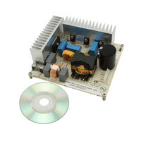
EVAL BOARD FOR L6563(400W)
Manufacturer
STMicroelectronics
Type
Motor / Motion Controllers & Driversr
Specifications of EVL6563S-400W
Main Purpose
Power Management, Power Factor Correction
Embedded
No
Utilized Ic / Part
L6563
Primary Attributes
400W Power Factor Correction and Preregulator Combination
Secondary Attributes
Transition Mode & Active Tracking Boost Function.
Maximum Operating Temperature
+ 60 C
Product
Power Management Development Tools
Lead Free Status / RoHS Status
Lead free / RoHS Compliant
For Use With/related Products
L6563S
Other names
497-10488
Available stocks
Company
Part Number
Manufacturer
Quantity
Price


Layout hints
3
26/38
Layout hints
The layout of any converter is a very important phase in the design process that sometimes
does not get the required attention by engineers. Even if the layout phase is sometimes
time-consuming, a good layout saves time during the functional debugging and qualification
phases. Additionally, a power supply circuit with a correct layout needs smaller EMI filters or
less filter stages and therefore contributes to money saving.
The L6563S does not require any specific attention to the layout. General layout rules for
any power converter have to be applied carefully. These basic rules are listed below, taking
the EVL6563S-400W schematic as reference. They can be used for other PFC circuits with
any power level, working either in FOT or TM control mode.
1.
2.
3.
4.
5.
6.
7.
Keep the power and signal RTN separate. Connect the return pins of the component
carrying the high current, such as the C4, C5 input filter, sense resistors, C6 and C7
output capacitor, as close as possible. This point will be the RTN’s start point. A
downstream converter will have to be connected to this return point.
Minimize the length of the traces relevant to L3, boost inductor L4, MOSFET drain,
boost rectifier D4 and output capacitors C6 and C7.
Keep signal components as close as possible to each relevant pin of the L6563S. Keep
the tracks relevant to pin #1 (INV) as short as possible. Components and traces
relevant to the error amplifier have to be placed far from traces and connections
carrying signals with high dv/dt like the MOSFET drains (Q1 and Q2).
Connect heat sinks to the power GND.
Add an external shield to the boost inductor and connect it to the power GND.
Connect the RTN of the signal components, including the feedback, PFC_OK and
MULT dividers, close to the L6563S’ pin #12 (GND).
Connect a ceramic capacitor (100÷470 nF) to pin #14 (Vcc) and to pin #12 (GND),
close to the L6563S. Connect this point to the RTN’s start point (see 1).
Doc ID 15796 Rev 2
AN2994
Related parts for EVL6563S-400W
Image
Part Number
Description
Manufacturer
Datasheet
Request
R

Part Number:
Description:
EVAL BOARD FOR L6563(100W)
Manufacturer:
STMicroelectronics
Datasheet:

Part Number:
Description:
EVAL BOARD FOR L6563(250W)
Manufacturer:
STMicroelectronics
Datasheet:

Part Number:
Description:
Power Management Modules & Development Tools Tranisition Mode PFC L6563S EVL Board
Manufacturer:
STMicroelectronics
Datasheet:

Part Number:
Description:
EVAL BOARD L6563 (200W)
Manufacturer:
STMicroelectronics
Datasheet:
Part Number:
Description:
STMicroelectronics [RIPPLE-CARRY BINARY COUNTER/DIVIDERS]
Manufacturer:
STMicroelectronics
Datasheet:
Part Number:
Description:
STMicroelectronics [LIQUID-CRYSTAL DISPLAY DRIVERS]
Manufacturer:
STMicroelectronics
Datasheet:

Part Number:
Description:
BOARD EVAL FOR MEMS SENSORS
Manufacturer:
STMicroelectronics
Datasheet:
Part Number:
Description:
NPN TRANSISTOR POWER MODULE
Manufacturer:
STMicroelectronics
Datasheet:
Part Number:
Description:
TURBOSWITCH ULTRA-FAST HIGH VOLTAGE DIODE
Manufacturer:
STMicroelectronics
Datasheet:
Part Number:
Description:
Manufacturer:
STMicroelectronics
Datasheet:
Part Number:
Description:
DIODE / SCR MODULE
Manufacturer:
STMicroelectronics
Datasheet:
Part Number:
Description:
DIODE / SCR MODULE
Manufacturer:
STMicroelectronics
Datasheet: