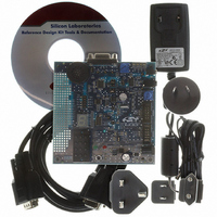
DTMFDECODER-RD Silicon Laboratories Inc, DTMFDECODER-RD Datasheet - Page 106
DTMFDECODER-RD
Manufacturer Part Number
DTMFDECODER-RD
Description
KIT REF DESIGN DTMF DECODER
Manufacturer
Silicon Laboratories Inc
Specifications of DTMFDECODER-RD
Mfg Application Notes
DTMF Decoder Ref Design AppNote
Main Purpose
Telecom, DTMF Decoder
Embedded
No
Utilized Ic / Part
C8051F300
Primary Attributes
8kHz Sampling Rate ADC
Secondary Attributes
16 Goertzel Filters
Processor To Be Evaluated
C8051F300
Interface Type
RS-232
Lead Free Status / RoHS Status
Contains lead / RoHS non-compliant
Lead Free Status / RoHS Status
Lead free / RoHS Compliant, Contains lead / RoHS non-compliant
Other names
336-1283


C8051F300/1/2/3/4/5
12.2. Port I/O Initialization
Port I/O initialization consists of the following steps:
All Port pins must be configured as either analog or digital inputs. Any pins to be used as Comparator or
ADC inputs should be configured as an analog inputs. When a pin is configured as an analog input, its
weak pull-up, digital driver, and digital receiver is disabled. This process saves power and reduces noise
on the analog input. Pins configured as digital inputs may still be used by analog peripherals; however this
practice is not recommended.
Additionally, all analog input pins should be configured to be skipped by the Crossbar (accomplished by
setting the associated bits in XBR0). Port input mode is set in the P0MDIN register, where a ‘1’ indicates a
digital input, and a ‘0’ indicates an analog input. All pins default to digital inputs on reset. See SFR Defini-
tion 12.5 for the P0MDIN register details.
The output driver characteristics of the I/O pins are defined using the Port0 Output Mode register
P0MDOUT (see SFR Definition 12.6). Each Port Output driver can be configured as either open drain or
push-pull. This selection is required even for the digital resources selected in the XBRn registers, and is
not automatic. The only exception to this is the SMBus (SDA, SCL) pins, which are configured as open-
drain regardless of the P0MDOUT settings. When the WEAKPUD bit in XBR2 is ‘0’, a weak pull-up is
enabled for all Port I/O configured as open-drain. WEAKPUD does not affect the push-pull Port I/O. Fur-
thermore, the weak pull-up is turned off on an open-drain output that is driving a ‘0’ to avoid unnecessary
power dissipation.
Registers XBR0, XBR1 and XBR2 must be loaded with the appropriate values to select the digital I/O func-
tions required by the design. Setting the XBARE bit in XBR2 to ‘1’ enables the Crossbar. Until the Crossbar
is enabled, the external pins remain as standard digital inputs (output drivers disabled) regardless of the
XBRn Register settings. For given XBRn Register settings, one can determine the I/O pin-out using the
Priority Decode Table; as an alternative, the Configuration Wizard utility of the Silicon Labs IDE software
will determine the Port I/O pin assignments based on the XBRn Register settings.
106
Step 1. Select the input mode (analog or digital) for all Port pins, using the Port0 Input Mode
Step 2. Select the output mode (open-drain or push-pull) for all Port pins, using the Port0 Output
Step 3. Set XBR0 to skip any pins selected as analog inputs or special functions.
Step 4. Assign Port pins to desired peripherals.
Step 5. Enable the Crossbar.
Mode register (P0MDOUT).
register (P0MDIN).
Rev. 2.9
Related parts for DTMFDECODER-RD
Image
Part Number
Description
Manufacturer
Datasheet
Request
R

Part Number:
Description:
SMD/C°/SINGLE-ENDED OUTPUT SILICON OSCILLATOR
Manufacturer:
Silicon Laboratories Inc
Part Number:
Description:
Manufacturer:
Silicon Laboratories Inc
Datasheet:
Part Number:
Description:
N/A N/A/SI4010 AES KEYFOB DEMO WITH LCD RX
Manufacturer:
Silicon Laboratories Inc
Datasheet:
Part Number:
Description:
N/A N/A/SI4010 SIMPLIFIED KEY FOB DEMO WITH LED RX
Manufacturer:
Silicon Laboratories Inc
Datasheet:
Part Number:
Description:
N/A/-40 TO 85 OC/EZLINK MODULE; F930/4432 HIGH BAND (REV E/B1)
Manufacturer:
Silicon Laboratories Inc
Part Number:
Description:
EZLink Module; F930/4432 Low Band (rev e/B1)
Manufacturer:
Silicon Laboratories Inc
Part Number:
Description:
I°/4460 10 DBM RADIO TEST CARD 434 MHZ
Manufacturer:
Silicon Laboratories Inc
Part Number:
Description:
I°/4461 14 DBM RADIO TEST CARD 868 MHZ
Manufacturer:
Silicon Laboratories Inc
Part Number:
Description:
I°/4463 20 DBM RFSWITCH RADIO TEST CARD 460 MHZ
Manufacturer:
Silicon Laboratories Inc
Part Number:
Description:
I°/4463 20 DBM RADIO TEST CARD 868 MHZ
Manufacturer:
Silicon Laboratories Inc
Part Number:
Description:
I°/4463 27 DBM RADIO TEST CARD 868 MHZ
Manufacturer:
Silicon Laboratories Inc
Part Number:
Description:
I°/4463 SKYWORKS 30 DBM RADIO TEST CARD 915 MHZ
Manufacturer:
Silicon Laboratories Inc
Part Number:
Description:
N/A N/A/-40 TO 85 OC/4463 RFMD 30 DBM RADIO TEST CARD 915 MHZ
Manufacturer:
Silicon Laboratories Inc
Part Number:
Description:
I°/4463 20 DBM RADIO TEST CARD 169 MHZ
Manufacturer:
Silicon Laboratories Inc