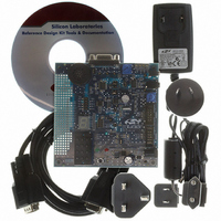
DTMFDECODER-RD Silicon Laboratories Inc, DTMFDECODER-RD Datasheet - Page 143
DTMFDECODER-RD
Manufacturer Part Number
DTMFDECODER-RD
Description
KIT REF DESIGN DTMF DECODER
Manufacturer
Silicon Laboratories Inc
Specifications of DTMFDECODER-RD
Mfg Application Notes
DTMF Decoder Ref Design AppNote
Main Purpose
Telecom, DTMF Decoder
Embedded
No
Utilized Ic / Part
C8051F300
Primary Attributes
8kHz Sampling Rate ADC
Secondary Attributes
16 Goertzel Filters
Processor To Be Evaluated
C8051F300
Interface Type
RS-232
Lead Free Status / RoHS Status
Contains lead / RoHS non-compliant
Lead Free Status / RoHS Status
Lead free / RoHS Compliant, Contains lead / RoHS non-compliant
Other names
336-1283


15. Timers
Each MCU includes 3 counter/timers: two are 16-bit counter/timers compatible with those found in the
standard 8051, and one is a 16-bit auto-reload timer for use with the ADC, SMBus, or for general purpose
use. These timers can be used to measure time intervals, count external events and generate periodic
interrupt requests. Timer 0 and Timer 1 are nearly identical and have four primary modes of operation.
Timer 2 offers 16-bit and split 8-bit timer functionality with auto-reload.
Timers 0 and 1 may be clocked by one of five sources, determined by the Timer Mode Select bits
(T1M–T0M) and the Clock Scale bits (SCA1–SCA0). The Clock Scale bits define a pre-scaled clock from
which Timer 0 and/or Timer 1 may be clocked (See SFR Definition 15.3 for pre-scaled clock selection).
Timer 0/1 may then be configured to use this pre-scaled clock signal or the system clock. Timer 2 may be
clocked by the system clock, the system clock divided by 12, or the external oscillator clock source divided
by 8.
Timer 0 and Timer 1 may also be operated as counters. When functioning as a counter, a counter/timer
register is incremented on each high-to-low transition at the selected input pin. Events with a frequency of
up to one-fourth the system clock's frequency can be counted. The input signal need not be periodic, but it
should be held at a given level for at least two full system clock cycles to ensure the level is properly sam-
pled.
15.1. Timer 0 and Timer 1
Each timer is implemented as 16-bit register accessed as two separate bytes: a low byte (TL0 or TL1) and
a high byte (TH0 or TH1). The Counter/Timer Control register (TCON) is used to enable Timer 0 and Timer
1 as well as indicate their status. Timer 0 interrupts can be enabled by setting the ET0 bit in the IE register
(Section “8.3.5. Interrupt Register Descriptions” on page
setting the ET1 bit in the IE register
modes selected by setting the Mode Select bits T1M1–T0M0 in the Counter/Timer Mode register (TMOD).
Each timer can be configured independently. Each operating mode is described below.
15.1.1. Mode 0: 13-bit Counter/Timer
Timer 0 and Timer 1 operate as 13-bit counter/timers in Mode 0. The following describes the configuration
and operation of Timer 0. However, both timers operate identically, and Timer 1 is configured in the same
manner as described for Timer 0.
The TH0 register holds the eight MSBs of the 13-bit counter/timer. TL0 holds the five LSBs in bit positions
TL0.4-TL0.0. The three upper bits of TL0 (TL0.7-TL0.5) are indeterminate and should be masked out or
ignored when reading. As the 13-bit timer register increments and overflows from 0x1FFF (all ones) to
0x0000, the timer overflow flag TF0 (TCON.5) is set and an interrupt will occur if Timer 0 interrupts are
enabled.
Two 8-bit counter/timers (Timer 0 only)
8-bit counter/timer with auto-reload
Timer 0 and Timer 1 Modes:
13-bit counter/timer
16-bit counter/timer
(Section
8.3.5). Both counter/timers operate in one of four primary
Rev. 2.9
Two 8-bit timers with auto-reload
16-bit timer with auto-reload
75); Timer 1 interrupts can be enabled by
C8051F300/1/2/3/4/5
Timer 2 Modes:
143
Related parts for DTMFDECODER-RD
Image
Part Number
Description
Manufacturer
Datasheet
Request
R

Part Number:
Description:
SMD/C°/SINGLE-ENDED OUTPUT SILICON OSCILLATOR
Manufacturer:
Silicon Laboratories Inc
Part Number:
Description:
Manufacturer:
Silicon Laboratories Inc
Datasheet:
Part Number:
Description:
N/A N/A/SI4010 AES KEYFOB DEMO WITH LCD RX
Manufacturer:
Silicon Laboratories Inc
Datasheet:
Part Number:
Description:
N/A N/A/SI4010 SIMPLIFIED KEY FOB DEMO WITH LED RX
Manufacturer:
Silicon Laboratories Inc
Datasheet:
Part Number:
Description:
N/A/-40 TO 85 OC/EZLINK MODULE; F930/4432 HIGH BAND (REV E/B1)
Manufacturer:
Silicon Laboratories Inc
Part Number:
Description:
EZLink Module; F930/4432 Low Band (rev e/B1)
Manufacturer:
Silicon Laboratories Inc
Part Number:
Description:
I°/4460 10 DBM RADIO TEST CARD 434 MHZ
Manufacturer:
Silicon Laboratories Inc
Part Number:
Description:
I°/4461 14 DBM RADIO TEST CARD 868 MHZ
Manufacturer:
Silicon Laboratories Inc
Part Number:
Description:
I°/4463 20 DBM RFSWITCH RADIO TEST CARD 460 MHZ
Manufacturer:
Silicon Laboratories Inc
Part Number:
Description:
I°/4463 20 DBM RADIO TEST CARD 868 MHZ
Manufacturer:
Silicon Laboratories Inc
Part Number:
Description:
I°/4463 27 DBM RADIO TEST CARD 868 MHZ
Manufacturer:
Silicon Laboratories Inc
Part Number:
Description:
I°/4463 SKYWORKS 30 DBM RADIO TEST CARD 915 MHZ
Manufacturer:
Silicon Laboratories Inc
Part Number:
Description:
N/A N/A/-40 TO 85 OC/4463 RFMD 30 DBM RADIO TEST CARD 915 MHZ
Manufacturer:
Silicon Laboratories Inc
Part Number:
Description:
I°/4463 20 DBM RADIO TEST CARD 169 MHZ
Manufacturer:
Silicon Laboratories Inc