DTMFDECODER-RD Silicon Laboratories Inc, DTMFDECODER-RD Datasheet - Page 161
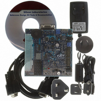
DTMFDECODER-RD
Manufacturer Part Number
DTMFDECODER-RD
Description
KIT REF DESIGN DTMF DECODER
Manufacturer
Silicon Laboratories Inc
Specifications of DTMFDECODER-RD
Mfg Application Notes
DTMF Decoder Ref Design AppNote
Main Purpose
Telecom, DTMF Decoder
Embedded
No
Utilized Ic / Part
C8051F300
Primary Attributes
8kHz Sampling Rate ADC
Secondary Attributes
16 Goertzel Filters
Processor To Be Evaluated
C8051F300
Interface Type
RS-232
Lead Free Status / RoHS Status
Contains lead / RoHS non-compliant
Lead Free Status / RoHS Status
Lead free / RoHS Compliant, Contains lead / RoHS non-compliant
Other names
336-1283


16.2.4. Frequency Output Mode
Frequency Output Mode produces a programmable-frequency square wave on the module’s associated
CEXn pin. The capture/compare module high byte holds the number of PCA clocks to count before the out-
put is toggled. The frequency of the square wave is then defined by Equation 16.1.
Where F
PCA0MD. The lower byte of the capture/compare module is compared to the PCA counter low byte; on a
match, CEXn is toggled and the offset held in the high byte is added to the matched value in PCA0CPLn.
Frequency Output Mode is enabled by setting the ECOMn, TOGn, and PWMn bits in the PCA0CPMn reg-
ister.
PCA0CPLn
Write to
Reset
PCA
PCA0CPHn
Write to
is the frequency of the clock selected by the CPS2–0 bits in the PCA mode register,
0
1
ENB
ENB
Equation 16.1. Square Wave Frequency Output
Figure 16.7. PCA Frequency Output Mode
W
M
P
1
6
n
x
O
M
E
C
n
PCA0CPMn
C
A
P
P
n
0 0 0
C
N
A
P
n
M
A
T
n
O
G
T
n
W
M
P
n
C
C
E
F
n
x
PCA Timebase
F
CEXn
Enable
=
Comparator
PCA0CPLn
Rev. 2.9
---------------------------------------- -
2
PCA0L
8-bit
PCA0CPHn
F
PCA
match
C8051F300/1/2/3/4/5
Enable
Adder
8-bit Adder
Toggle
TOGn
0
1
CEXn
PCA0CPHn
Crossbar
Port I/O
161
Related parts for DTMFDECODER-RD
Image
Part Number
Description
Manufacturer
Datasheet
Request
R

Part Number:
Description:
SMD/C°/SINGLE-ENDED OUTPUT SILICON OSCILLATOR
Manufacturer:
Silicon Laboratories Inc
Part Number:
Description:
Manufacturer:
Silicon Laboratories Inc
Datasheet:
Part Number:
Description:
N/A N/A/SI4010 AES KEYFOB DEMO WITH LCD RX
Manufacturer:
Silicon Laboratories Inc
Datasheet:
Part Number:
Description:
N/A N/A/SI4010 SIMPLIFIED KEY FOB DEMO WITH LED RX
Manufacturer:
Silicon Laboratories Inc
Datasheet:
Part Number:
Description:
N/A/-40 TO 85 OC/EZLINK MODULE; F930/4432 HIGH BAND (REV E/B1)
Manufacturer:
Silicon Laboratories Inc
Part Number:
Description:
EZLink Module; F930/4432 Low Band (rev e/B1)
Manufacturer:
Silicon Laboratories Inc
Part Number:
Description:
I°/4460 10 DBM RADIO TEST CARD 434 MHZ
Manufacturer:
Silicon Laboratories Inc
Part Number:
Description:
I°/4461 14 DBM RADIO TEST CARD 868 MHZ
Manufacturer:
Silicon Laboratories Inc
Part Number:
Description:
I°/4463 20 DBM RFSWITCH RADIO TEST CARD 460 MHZ
Manufacturer:
Silicon Laboratories Inc
Part Number:
Description:
I°/4463 20 DBM RADIO TEST CARD 868 MHZ
Manufacturer:
Silicon Laboratories Inc
Part Number:
Description:
I°/4463 27 DBM RADIO TEST CARD 868 MHZ
Manufacturer:
Silicon Laboratories Inc
Part Number:
Description:
I°/4463 SKYWORKS 30 DBM RADIO TEST CARD 915 MHZ
Manufacturer:
Silicon Laboratories Inc
Part Number:
Description:
N/A N/A/-40 TO 85 OC/4463 RFMD 30 DBM RADIO TEST CARD 915 MHZ
Manufacturer:
Silicon Laboratories Inc
Part Number:
Description:
I°/4463 20 DBM RADIO TEST CARD 169 MHZ
Manufacturer:
Silicon Laboratories Inc