DTMFDECODER-RD Silicon Laboratories Inc, DTMFDECODER-RD Datasheet - Page 50
DTMFDECODER-RD
Manufacturer Part Number
DTMFDECODER-RD
Description
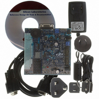
KIT REF DESIGN DTMF DECODER
Manufacturer
Silicon Laboratories Inc
Specifications of DTMFDECODER-RD
Mfg Application Notes
DTMF Decoder Ref Design AppNote
Main Purpose
Telecom, DTMF Decoder
Embedded
No
Utilized Ic / Part
C8051F300
Primary Attributes
8kHz Sampling Rate ADC
Secondary Attributes
16 Goertzel Filters
Processor To Be Evaluated
C8051F300
Interface Type
RS-232
Lead Free Status / RoHS Status
Contains lead / RoHS non-compliant
Lead Free Status / RoHS Status
Lead free / RoHS Compliant, Contains lead / RoHS non-compliant
Other names
336-1283


C8051F300/1/2/3/4/5
Table 6.1. External Voltage Reference Circuit Electrical Characteristics
V
50
DD
Bits7–3: UNUSED. Read = 00000b; Write = don’t care.
Bit3:
Bit2:
Bit1:
Bit0:
Input Voltage Range
= 3.0 V; –40 to +85°C unless otherwise specified.
R/W
Bit7
—
Input Current
Parameter
REFSL: Voltage Reference Select.
This bit selects the source for the internal voltage reference.
0: VREF input pin used as voltage reference.
1: V
TEMPE: Temperature Sensor Enable Bit.
0: Internal Temperature Sensor off.
1: Internal Temperature Sensor on.
BIASE: Internal Analog Bias Generator Enable Bit. (Must be ‘1’ if using ADC).
0: Internal Bias Generator off.
1: Internal Bias Generator on.
UNUSED. Read = 0b. Write = don’t care.
DD
SFR Definition 6.1.
R/W
Bit6
—
used as voltage reference.
R/W
Bit5
—
Sample Rate = 500 ksps;
R/W
Bit4
—
VREF = 3.0 V
REF0CN: Reference Control Register
Conditions
REFSL
Rev. 2.9
R/W
Bit3
TEMPE
R/W
Bit2
Min
—
0
BIASE
R/W
Bit1
Typ
12
—
R/W
Bit0
—
Max
V
—
DD
SFR Address:
00000000
Reset Value
0xD1
Units
µA
V
Related parts for DTMFDECODER-RD
Image
Part Number
Description
Manufacturer
Datasheet
Request
R

Part Number:
Description:
SMD/C°/SINGLE-ENDED OUTPUT SILICON OSCILLATOR
Manufacturer:
Silicon Laboratories Inc
Part Number:
Description:
Manufacturer:
Silicon Laboratories Inc
Datasheet:
Part Number:
Description:
N/A N/A/SI4010 AES KEYFOB DEMO WITH LCD RX
Manufacturer:
Silicon Laboratories Inc
Datasheet:
Part Number:
Description:
N/A N/A/SI4010 SIMPLIFIED KEY FOB DEMO WITH LED RX
Manufacturer:
Silicon Laboratories Inc
Datasheet:
Part Number:
Description:
N/A/-40 TO 85 OC/EZLINK MODULE; F930/4432 HIGH BAND (REV E/B1)
Manufacturer:
Silicon Laboratories Inc
Part Number:
Description:
EZLink Module; F930/4432 Low Band (rev e/B1)
Manufacturer:
Silicon Laboratories Inc
Part Number:
Description:
I°/4460 10 DBM RADIO TEST CARD 434 MHZ
Manufacturer:
Silicon Laboratories Inc
Part Number:
Description:
I°/4461 14 DBM RADIO TEST CARD 868 MHZ
Manufacturer:
Silicon Laboratories Inc
Part Number:
Description:
I°/4463 20 DBM RFSWITCH RADIO TEST CARD 460 MHZ
Manufacturer:
Silicon Laboratories Inc
Part Number:
Description:
I°/4463 20 DBM RADIO TEST CARD 868 MHZ
Manufacturer:
Silicon Laboratories Inc
Part Number:
Description:
I°/4463 27 DBM RADIO TEST CARD 868 MHZ
Manufacturer:
Silicon Laboratories Inc
Part Number:
Description:
I°/4463 SKYWORKS 30 DBM RADIO TEST CARD 915 MHZ
Manufacturer:
Silicon Laboratories Inc
Part Number:
Description:
N/A N/A/-40 TO 85 OC/4463 RFMD 30 DBM RADIO TEST CARD 915 MHZ
Manufacturer:
Silicon Laboratories Inc
Part Number:
Description:
I°/4463 20 DBM RADIO TEST CARD 169 MHZ
Manufacturer:
Silicon Laboratories Inc