DEMOBOARD TLE8201R Infineon Technologies, DEMOBOARD TLE8201R Datasheet
DEMOBOARD TLE8201R
Specifications of DEMOBOARD TLE8201R


Related parts for DEMOBOARD TLE8201R


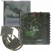
DEMOBOARD TLE8201R Summary of contents
Page 1
Door Module Power IC TLE 8201R Data Sheet Rev. 2.0 Features • Full bridge (150m ) for main doorlock motor • Two half-bridges (400m ) for deadbolt and mirror position motor or mirror fold motor • Two half-bridges (800m ) ...
Page 2
Table of Contents 1 Block Diagram . . . . . . . . . . . . . . . . . . . . . . . . . . . . . . . . . . ...
Page 3
Block Diagram Vcc INH CSN CLK DI DO PWM1 PWM2 ISO sense MUX OUT8 OUT9 OUT10 OUT11 Figure 1 Block Diagram Data Sheet Rev. 2 Charge- pump Biasing RevPol MOS driver Fault- Detect SPI Logic and ...
Page 4
Pin Configuration 2.1 Pin Assignment GND 1 OUT5 2 3 OUT6 4 Vs INH 5 6 PWM1 7 PWM2 ISO 8 9 Vcc DO 10 CLK 11 CSN OUT1 16 OUT1 17 ...
Page 5
Pin Definitions and Functions Pin Symbol Function cooling GND Cooling tab, internally connected to GND; to reduce thermal tab resistance place cooling areas and thermal vias on PCB. 1, 18, GND Ground; internally connected to cooling tab (heat slug). ...
Page 6
Pin Symbol Function 13 DI Serial Data Input; Receives serial data from the master when the chip is selected by CSN=LOW. Data transmission is synchronized by CLK. Data are accepted on the falling edge of CLK. The LSB is transferred ...
Page 7
Electrical Characteristics 3.1 Absolute Maximum Ratings Pos. Parameter 3.1.1 Supply voltage 3.1.2 Logic supply Voltage 3.1.3 Logic input- and output Voltages 3.1.4 Voltage at GO-pin 3.1.5 Junction temperature 3.1.6 Storage temperature 3.1.7 ESD capability of power stage output and ...
Page 8
Operating Range Pos. Parameter 3.2.1 Supply voltage 3.2.2 Supply voltage 3.2.3 Supply voltage 3.2.4 Logic supply voltage 3.2.5 SPI clock frequency 3.2.6 Junction temperature Note: Within the functional range the IC operates as described in the circuit description. The ...
Page 9
Block Description and Electrical Characteristics 4.1 Power Supply 4.1.1 General The TLE 8201R has two power supply inputs: All power drivers are connected to the V supply voltage which is connected to the automotive 12 V board-net. The internal ...
Page 10
Electrical Characteristics < < 4.75 V < -40 C < < 150 C; unless otherwise specified j Pos. Parameter 4.1.3 Quiescent current 4.1.4 Logic quiescent current 4.1.5 Total quiescent current Charge Pump-output for ...
Page 11
Monitoring Functions 4.2.1 Power Supply Monitoring The power supply Voltage • Under Voltage If the supply voltage transistors are switched off and the power supply fail bit PSF is set. The error is not V latched, i.e. if rises ...
Page 12
Temperature Monitoring Temperature sensors are integrated in the power stages. The temperature monitoring circuit compares the measured temperature to the warning and shutdown thresholds. If one or more temperature sensors reach the warning temperature, the temperature warning bit TW ...
Page 13
Current Sense A current proportional to the output current that flows from the selected power output to GND is provided at the ISO (I sense out) pin. The output selection is done via the SPI. The sense current can ...
Page 14
SPI 4.3.1 General The SPI is used for bidirectional communication with a control unit. The TLE 8201R acts as SPI-slave and the control unit acts as SPI-master. The 16-bit control word is read via the DI serial data input. ...
Page 15
H ->L), the diagnostic data currently valid are latched into the SPI and transferred to the master. For Status Register address handling, please refer to CSN bit DI Data for selected register address DO Data from selected ...
Page 16
SPI bit definitions 4.3.3.1 Control - word Table 1 Input (Control) Data Register Bit CtrlReg 00 Lock and Mirror heat control 15 LS1ON 14 HS1ON 13 LS2ON 12 HS2ON 11 LS3ON 10 HS3ON 9 HS7ON 8 Testmode 7 Testmode ...
Page 17
Table 2 Control bit definitions Control Bit Definition LSxON low-side switch no turned ON (OFF) if this bit is set to HIGH (LOW) HSxON high-side switch no turned ON (OFF) if this bit is set to ...
Page 18
Diagnosis Table 3 Output (Status) Data Register Bit StatReg 00 Lock and Mirror heat overload valid for input data LS1OvL 14 HS1OvL 13 LS2OvL 12 HS2OvL 11 LS3OvL 10 HS3OvL 9 HS7OvL 8 n.c. 7 ...
Page 19
Table 4 Status bit definitions Status Bit Definition LSxOvL Low-Side switch Over Load. Set to HIGH if low-side switch no shut down due to overcurrent or over temperature HSxOvL High-Side switch Over Load. Set to HIGH if high-side ...
Page 20
Status Register Address selection and Reset The SPI is using a standard shift-register concept with daisy-chain capability. Any data transmitted to the SPI will be available to the internal logic part at the end of the SPI transmission (CSN ...
Page 21
Error-Flag In addition to the 16 bits transferred from the TLE 7201R to the SPI master, an additional Error Flag (EF) is transmitted at the DO pin. The EF status is shown on the DO pin after CSN H->L, ...
Page 22
Electrical Characteristics - SPI-timing < < 4.75 V < -40 C < < 150 C; unless otherwise specified j Pos. Parameter 4.3.5 DI data setup time 4.3.6 DI data hold time 4.3.7 DI ...
Page 23
Stage x, xsel1 and xsel2 are LOW, the power stage x is controlled only via the SPI control bit xON. If the selection bit xsel1 is HIGH and the control bit xON is also high, the power stage x ...
Page 24
Truth-table for PWM inputs xON xsel1 xsel2 Data Sheet Rev. 2.0 PWM1 PWM2 ...
Page 25
Power-Outputs 1-6 (Bridge Outputs) 4.4.1 Protection and Diagnosis 4.4.1.1 Short Circuit of Output to Ground or Vs The low-side switches are protected against short circuit to supply and the high-side switches against short to GND switch is ...
Page 26
Open Load Open-load detection in ON-state is implemented in the low-side switches of the bridge outputs: When the current through the low side transistor is lower than the reference I current in ON-state for longer than the open-load detection ...
Page 27
Electrical Characteristics Electrical Characteristics OUT 1 and 2 (driver for door latch < < 4.75 V < -40 C < < 150 C; unless otherwise specified j Pos. Parameter Static Drain-source ON-Resistance ...
Page 28
Electrical Characteristics OUT3, 4 (Driver for deadbolt, mirror fold and mirror xy < < 4.75 V < -40 C < < 150 C; unless otherwise specified j Pos. Parameter Static Drain-source ON-Resistance 4.4.14 ...
Page 29
Electrical Characteristics OUT 5, 6 (driver for mirror x-y position < < 4.75 V < -40 C < < 150 C; unless otherwise specified j Pos. Parameter Static Drain-source ON-Resistance 4.4.27 High- and ...
Page 30
ON -> OFF OFF OFF OFF -> ON Figure 11 Timing bridge outputs high to low OFF ON -> OFF OFF -> ON OFF Figure 12 Timing bridge outputs low to high Data Sheet Rev. 2.0 CSN OUTx t dO ...
Page 31
Power-Output 7 (Mirror heater driver) Output high-side switch intended to drive ohmic loads like the heater of an exterior mirror. 4.5.1 Protection and Diagnosis 4.5.1.1 Short Circuit of Output to Ground If the high-side switch is ...
Page 32
OpL7ON switch ON HS7 HS7OpL Filter Figure 14 Open load in OFF-state scheme Data Sheet Rev. 2.0 Gate driver 1 & TLE 8201R I OpL OUT 7 high-side switch 7 R Load + V OpL - 2006-06-07 ...
Page 33
Electrical Characteristics Electrical Characteristics OUT 7 (mirror heater driver < < 4.75 V < -40 C < < 150 C; unless otherwise specified j Pos. Parameter Static Drain-source ON-Resistance 4.5.1 High-side switch ...
Page 34
PWM PWM OUT7 Figure 15 Timing OUT 7 Data Sheet Rev. 2 ISE 90% 90 dON dOFF 10% 34 TLE 8201R t FALL 10% 2006-06-07 ...
Page 35
Power-Outputs (Lamp drivers) Outputs are a high-side switches intended to drive ohmic loads 5W or 10W lamp (bulb) loads. 4.6.1 Protection and Diagnosis 4.6.1.1 Short Circuit of Output to Ground The high-side switches ...
Page 36
Short Circuit in On-state If a switch is already on and the current rises above the shutdown threshold longer than the shutdown delay time corresponding diagnosis bit is set. This is independent of the voltage V Figure 17 OUT 8...11 ...
Page 37
OpLxON switch ON HSx HSxOpL Filter Figure 18 Open load in OFF-state scheme Data Sheet Rev. 2.0 Gate driver 1 & TLE 8201R I OpL OUT x high-side switch 7 R Load + V - OpL 2006-06-07 ...
Page 38
Electrical Characteristics Electrical Characteristics OUT (Lamp drivers < < 4.75 V < -40 C < < 150 C; unless otherwise specified j Pos. Parameter Static Drain-source ON-Resistance 4.6.1 High-side ...
Page 39
PWM PWM OUT8-11 Figure 19 Timing OUT Data Sheet Rev. 2.0 t RISE 90% 90 dON dOFF 10% 39 TLE 8201R t FALL 10% 2006-06-07 ...
Page 40
Logic In- and Outputs The threshold specifications of the logic inputs are compatible to both 5V and 3.3V standard CMOS micro controller outputs. The logic output CMOS output 4.7.1 Electrical Characteristics Electrical Characteristics Diagnostics V ...
Page 41
Application Description Vbat Vcc To 5V supply 10nF INH CSN CLK DI DO PWM1 PWM2 ISO Rsense 700 OUT8 OUT9 OUT10 OUT11 Figure 20 Application example with two-motor (safety-) lock Data Sheet Rev. 2.0 47uF // <40V 2 x ...
Page 42
Vbat Vcc To 5V supply 10nF INH CSN CLK DI DO PWM1 PWM2 ISO Rsense 700 OUT8 OUT9 OUT10 OUT11 Figure 21 Application example with mirror-fold Data Sheet Rev. 2.0 47uF // <40V 2 x 100nF GO Vs GND 42 ...
Page 43
Package Outlines PG-DSO-36-27 (Plastic Dual Small Outline Package) 1.1 ±0.1 0.65 +0.13 0.25 36 Index Marking 45˚ 1) Does not include plastic or metal protrusion of 0.15 max. per side You can find all of our ...
Page 44
... Infineon Technologies Office. Infineon Technologies Components may only be used in life-support devices or systems with the express written approval of Infineon Technologies failure of such components can reasonably be expected to cause the failure of that life-support device or system affect the safety or effectiveness of that device or system. Life support devices or systems are intended to be implanted in the human body support and/or maintain and sustain and/or protect human life ...
Page 45
Revision History TLE 8201R Revision History: Previous Version: Page Subjects (major changes since last revision) No changes Data Sheet Rev. 2.0 2006-06-07 Preliminary Data Sheet Rev. 1.0 45 TLE 8201R 2006-06-07 ...