EVAL-AD7877EBZ Analog Devices Inc, EVAL-AD7877EBZ Datasheet - Page 26
EVAL-AD7877EBZ
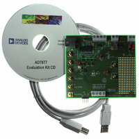
Manufacturer Part Number
EVAL-AD7877EBZ
Description
BOARD EVALUATION FOR AD7877
Manufacturer
Analog Devices Inc
Datasheets
1.AD7877ACBZ-REEL7.pdf
(44 pages)
2.EVAL-AD7877EBZ.pdf
(16 pages)
3.EVAL-AD7877EBZ.pdf
(44 pages)
Specifications of EVAL-AD7877EBZ
Main Purpose
Interface, Touch Screen Controller
Embedded
No
Utilized Ic / Part
AD7877
Primary Attributes
4-Wire Resistive Touch Screen Controller, SPI Interface, On-Chip: Temp Sensor, Voltage Reference, 8-Bit DAC
Secondary Attributes
USB GUI, LCD Noise Reduction Feature, 2.7 ~ 5.25 V, Wake Up on Touch Feature
Lead Free Status / RoHS Status
Lead free / RoHS Compliant


AD7877
8-BIT DAC
The AD7877 features an on-chip 8-bit DAC for LCD contrast
control. The DAC can be configured for voltage output by
clearing Bit 2 of the DAC register (Address 1110b), or for
current output by setting this bit.
The output voltage range can be set to 0 to V
Bit 0 of the DAC register, or to 0 to V
current mode, the output range is selectable by an external
resistor, R
This sets the full-scale output current according to the following
equations:
In current mode, the DAC sinks current, that is, positive
current flows into ground. The maximum output current is
1000 μA. The DAC is updated by writing to Address 1110b of
the DAC register. The 8 MSBs of the data-word are used for
DAC data.
The most effective way to control LCD contrast with the DAC is
to use it to control the feedback loop of the dc to dc converter
that supplies the LCD bias voltage, as shown in Figure 45. The
bias voltage for graphic LCDs is typically in the range of 20 V to
25 V, and the dc to dc converter usually has a feedback loop that
attenuates the output voltage and compares it with an internal
reference voltage.
The circuit operates as follows. If the DAC is in current mode
when the DAC output is zero, it has no effect on the feedback
loop. Regardless of what the DAC does, the feedback loop
maintains the voltage across R4, V
output voltage, V
As the DAC output is increased, it increases the feedback current,
so the voltage across R2 and, therefore, the output voltage also
increase. Note that the voltage across R3 does not change. This
is important for calculation of the adjustment range.
ARNG
R
RNG
I
therefore,
R
V
FS
RNG
REF
AD7877
1
= V
8-BIT
DAC
× (R2 + R3)/R3
= V
RNG
CC
Figure 45. Using the DAC to Adjust LCD Contrast
GND
, connected between the ARNG pin and GND.
/(R
CC
NOTES:
1
2
R
R1 IS REQUIRED ONLY IF DAC IS IN VOLTAGE MODE.
/(I
RNG
RNG
OUT
FS
IS REQUIRED ONLY IF DAC IS IN CURRENT MODE.
AOUT
× 6)
× 6)
, is
I
OUT
R1
R2
R3
2
V
FB
FB
, equal to V
CC
V
CONVERTER
by setting this bit. In
REF
DC-DC
CC
COMP
/2 by clearing
REF
, and the
V
OUT
TO LCD
Rev. B | Page 26 of 44
(5)
In current mode, it is quite easy to calculate the resistor values
to give the required adjustment range in V
following steps:
1.
2.
3.
4.
5.
6.
7.
Example:
1.
2.
3.
4.
5.
6.
In voltage mode, the circuit operation depends on whether the
maximum output voltage of the DAC exceeds the dc to dc
converter V
When the DAC output voltage is zero, it sinks the maximum
current through R1. The feedback current and, therefore, V
are at their maximum. As the DAC output voltage increases, the
Find the required maximum and minimum values of V
from the LCD manufacturer’s data
Decide on the current around the feedback loop. For
reasonable accuracy of the output voltage, this current
should be at least 100 times the input bias current of the
dc–dc converter’s comparator
Calculate R3 using the following equation:
Calculate R2 for the minimum value of V
DAC has no effect
Because the voltage across R3 does not change, subtract
V
minimum voltages across R2
Calculate the change in feedback current between
minimum and maximum output voltages
This is the required full-scale current of the DAC.
Calculate R
V
V
V
Allow 100 μA around the feedback loop
R3 = 1.25 V/100 μA = 12.5 kΩ
Use the nearest preferred value of 12 kΩ and recalculate
the feedback current as
I
R2 = (20 V − 1.25 V)/104 μA = 180 kΩ
ΔI = 23.75 V/180 kΩ − 18.75 V/180 kΩ = 28 μA
R
FB
RNG
CC
OUT(MIN)
REF
REF
R3 = V
R2 = R3(V
ΔI = V
= 1.25 V/12 kΩ = 104 μA
= 5 V
is 1.25 V
from V
= 5 V/(6 × 28 μA) = 30 kΩ
REF
is 20 V and V
R2(MAX)
.
FB
/I
RNG
OUTMAX
FB
OUT(MIN)
= V
from Equation 5
/R2 − V
REF
and V
− V
/I
OUT(MAX)
FB
R2(MIN)
REF
OUTMIN
)/V
/R2
REF
is 25 V
to get the maximum and
OUT
using the
OUT
, when the
OUT
OUT
Related parts for EVAL-AD7877EBZ
Image
Part Number
Description
Manufacturer
Datasheet
Request
R


Part Number:
Description:
BOARD EVAL FOR SI270X-A
Manufacturer:
Silicon Laboratories Inc
Datasheet:

Part Number:
Description:
BUCK CONV REF DESIGN KIT IP1201
Manufacturer:
International Rectifier
Datasheet:
Part Number:
Description:
BOARD DEMO SYNC DUAL BUCK CNVTER
Manufacturer:
International Rectifier
Datasheet:
Part Number:
Description:
BOARD DEMO SYNC BUCK CONVETER
Manufacturer:
International Rectifier
Datasheet:

Part Number:
Description:
EVALBOARD/EB Omnidirectional microphone - Analog
Manufacturer:
Analog Devices
Datasheet:
Part Number:
Description:
EVALBOARD/EB Omnidirectional microphone - Analog
Manufacturer:
Analog Devices
Datasheet:


Part Number:
Description:
BOARD EVAL LED DRIVER LT3756
Manufacturer:
Linear Technology
Datasheet:

Part Number:
Description:
BOARD EVAL FOR AD7741/7742
Manufacturer:
Analog Devices Inc
Datasheet:

Part Number:
Description:
±1.7g Dual-Axis IMEMS Accelerometer Evaluation Board
Manufacturer:
Analog Devices Inc
Datasheet:

Part Number:
Description:
IC MULTIPLIER ANALOG 8-SOIC T/R
Manufacturer:
Analog Devices Inc
Datasheet:

Part Number:
Description:
IC ANALOG MULTIPLIER 8-DIP
Manufacturer:
Analog Devices Inc
Datasheet:
Part Number:
Description:
IC ANALOG MULTIPLIER 8-SOIC
Manufacturer:
Analog Devices Inc
Datasheet:
Part Number:
Description:
IC ANALOG MULTIPLIER 8-DIP
Manufacturer:
Analog Devices Inc
Datasheet: