EVAL-AD7877EBZ Analog Devices Inc, EVAL-AD7877EBZ Datasheet - Page 32
EVAL-AD7877EBZ
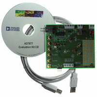
Manufacturer Part Number
EVAL-AD7877EBZ
Description
BOARD EVALUATION FOR AD7877
Manufacturer
Analog Devices Inc
Datasheets
1.AD7877ACBZ-REEL7.pdf
(44 pages)
2.EVAL-AD7877EBZ.pdf
(16 pages)
3.EVAL-AD7877EBZ.pdf
(44 pages)
Specifications of EVAL-AD7877EBZ
Main Purpose
Interface, Touch Screen Controller
Embedded
No
Utilized Ic / Part
AD7877
Primary Attributes
4-Wire Resistive Touch Screen Controller, SPI Interface, On-Chip: Temp Sensor, Voltage Reference, 8-Bit DAC
Secondary Attributes
USB GUI, LCD Noise Reduction Feature, 2.7 ~ 5.25 V, Wake Up on Touch Feature
Lead Free Status / RoHS Status
Lead free / RoHS Compliant


AD7877
GROUNDING AND LAYOUT
It is recommended that the ground pins, AGND and DGND, be
shorted together as close as possible to the device itself on the
user’s PCB.
For more information on grounding and layout considerations
for the AD7877, refer to the Layout and Grounding Recommen-
dations for Touch Screen Digitizers Technical Note.
PCB DESIGN GUIDELINES FOR CHIP SCALE
PACKAGES
The lands on the chip scale package (CP-32) are rectangular.
The printed circuit board pad for these should be 0.1 mm
longer than the package land length and 0.05 mm wider than
the package land width. To ensure that the solder joint size is
maximized, center the land on the pad.
SECONDARY
BATTERY
BATTERY
MAIN
REGULATOR
VOLTAGE
MEASUREMENT
TEMPERATURE
DIODE
REMOTE CONTROL
HOTSYNC INPUTS
FROM AUDIO
V
1.0μF–10μF
(OPTIONAL)
IN
CONVERTER
FROM
Figure 48. Typical Application Circuit
DC-DC
0.1μF
0.1μF
OUT
FB
Rev. B | Page 32 of 44
1
2
3
4
5
6
7
8
SCREEN
TOUCH
NC
BAT2
BAT1
AUX3/GPIO3
AUX2/GPIO2
AUX1/GPIO1
V
NC
CC
32
9
31
10
The bottom of the chip scale package has a central thermal pad.
The thermal pad on the printed circuit board should be at least
as large as this exposed pad. On the printed circuit board,
provide a clearance of at least 0.25 mm between the thermal pad
and the inner edges of the pad pattern to ensure that shorting is
avoided.
Using thermal vias on the printed circuit board thermal pad
improves the thermal performance of the package. If vias are
used, incorporate them in the thermal pad at a 1.2 mm pitch
grid. Keep the via diameter between 0.3 mm and 0.33 mm. The
via barrel should be plated with 1 oz. copper to plug the via.
The user should connect the printed circuit board thermal pad
to AGND.
11
30
AD7877
29
12
R
V
RNG
28
13
CC
14
27
TO LCD
BACKLIGHT
26
15
STOPACQ
NC = NO CONNECT
PENIRQ
ALERT
25
16
GPIO4
DAV
DIN
NC
CS
HSYNC SIGNAL
24
23
22
21
20
19
18
17
FROM LCD
GPIO
INT1
INT2
SCLK
MISO
MOSI
CS
PENIRQ
HOST
Related parts for EVAL-AD7877EBZ
Image
Part Number
Description
Manufacturer
Datasheet
Request
R


Part Number:
Description:
BOARD EVAL FOR SI270X-A
Manufacturer:
Silicon Laboratories Inc
Datasheet:

Part Number:
Description:
BUCK CONV REF DESIGN KIT IP1201
Manufacturer:
International Rectifier
Datasheet:
Part Number:
Description:
BOARD DEMO SYNC DUAL BUCK CNVTER
Manufacturer:
International Rectifier
Datasheet:
Part Number:
Description:
BOARD DEMO SYNC BUCK CONVETER
Manufacturer:
International Rectifier
Datasheet:

Part Number:
Description:
EVALBOARD/EB Omnidirectional microphone - Analog
Manufacturer:
Analog Devices
Datasheet:
Part Number:
Description:
EVALBOARD/EB Omnidirectional microphone - Analog
Manufacturer:
Analog Devices
Datasheet:


Part Number:
Description:
BOARD EVAL LED DRIVER LT3756
Manufacturer:
Linear Technology
Datasheet:

Part Number:
Description:
BOARD EVAL FOR AD7741/7742
Manufacturer:
Analog Devices Inc
Datasheet:

Part Number:
Description:
±1.7g Dual-Axis IMEMS Accelerometer Evaluation Board
Manufacturer:
Analog Devices Inc
Datasheet:

Part Number:
Description:
IC MULTIPLIER ANALOG 8-SOIC T/R
Manufacturer:
Analog Devices Inc
Datasheet:

Part Number:
Description:
IC ANALOG MULTIPLIER 8-DIP
Manufacturer:
Analog Devices Inc
Datasheet:
Part Number:
Description:
IC ANALOG MULTIPLIER 8-SOIC
Manufacturer:
Analog Devices Inc
Datasheet:
Part Number:
Description:
IC ANALOG MULTIPLIER 8-DIP
Manufacturer:
Analog Devices Inc
Datasheet: