EVAL-AD7877EBZ Analog Devices Inc, EVAL-AD7877EBZ Datasheet - Page 7
EVAL-AD7877EBZ
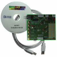
Manufacturer Part Number
EVAL-AD7877EBZ
Description
BOARD EVALUATION FOR AD7877
Manufacturer
Analog Devices Inc
Datasheets
1.AD7877ACBZ-REEL7.pdf
(44 pages)
2.EVAL-AD7877EBZ.pdf
(16 pages)
3.EVAL-AD7877EBZ.pdf
(44 pages)
Specifications of EVAL-AD7877EBZ
Main Purpose
Interface, Touch Screen Controller
Embedded
No
Utilized Ic / Part
AD7877
Primary Attributes
4-Wire Resistive Touch Screen Controller, SPI Interface, On-Chip: Temp Sensor, Voltage Reference, 8-Bit DAC
Secondary Attributes
USB GUI, LCD Noise Reduction Feature, 2.7 ~ 5.25 V, Wake Up on Touch Feature
Lead Free Status / RoHS Status
Lead free / RoHS Compliant


PIN CONFIGURATIONS AND FUNCTION DESCRIPTIONS
Table 4. Pin Function Descriptions
Pin No.
1, 8, 9, 16,
24, 25, 32
2
3
4
5
6
7
10
11
12
13
14
15
17
18
19
20
21
22
23
26
27
28
AUX3/GPIO3
AUX2/GPIO2
AUX1/GPIO1
NC = NO CONNECT
Mnemonic
NC
BAT2
BAT1
AUX3/GPIO3
AUX2/GPIO2
AUX1/GPIO1
V
X−
Y−
X+
Y+
AGND
DGND
PENIRQ
CS
DIN
STOPACQ
GPIO4
ALERT
DAV
DCLK
DOUT
V
BAT2
BAT1
V
CC
DRIVE
NC
NC
CC
Figure 4. LFCSP Pin Configuration
1
2
3
4
5
6
7
8
32
9
31
10
30
11
(Not to Scale)
Description
No Connect.
Battery Monitor Input. ADC Input Channel 7.
Battery Monitor Input. ADC Input Channel 6.
Auxiliary Analog Input. ADC Input Channel 5. Can be reconfigured as GPIO pin.
Auxiliary Analog Input. ADC Input Channel 4. Can be reconfigured as GPIO pin.
Auxiliary Analog Input. ADC Input Channel 3. Can be reconfigured as GPIO pin.
Power Supply Input. The V
Touch Screen Position Input.
Touch Screen Position Input. ADC Input Channel 2.
Touch Screen Position Input. ADC Input Channel 0.
Touch Screen Position Input. ADC Input Channel 1.
Analog Ground. Ground reference point for all analog circuitry on the AD7877. All analog input signals and any
external reference signal should be referred to this voltage.
Digital Ground. Ground reference for all digital circuitry on the AD7877. Refer all digital input signals to this
voltage.
Pen Interrupt. Digital active low output (has a 50 kΩ internal pull-up resistor).
Chip Select Input. Active low logic input. This input provides the dual function of initiating conversions on the
AD7877 and enabling the serial input/output register.
SPI® Serial Data Input. Data to be written to the AD7877 registers are provided on this input and clocked into
the register on the rising edge of DCLK.
Stop Acquisition Pin. A signal applied to this pin can be monitored by the AD7877, so that acquisition of new
data by the ADC is halted while the signal is active. Used to reduce the effect of noise from an LCD screen on
the touch screen measurements.
Dedicated General-Purpose Logic Input/Output Pin.
Digital Active Low Output. Interrupt output that goes low if a GPIO data bit is set, or if the AUX1, TEMP1, BAT1,
or BAT2 measurements are out of range.
Data Available Output. Active low logic output. Asserts low when new data is available in the AD7877 results
registers. This output is high impedance when CS is high.
External Clock Input. Logic input. DCLK provides the serial clock for accessing data from the part.
Serial Data Output. Logic output. The conversion result from the AD7877 is provided on this output as a serial
data stream. The bits are clocked out on the falling edge of the DCLK input. This output is high impedance
when CS is high.
Logic Power Supply Input. The voltage supplied at this pin determines the operating voltage for the serial
interface of the AD7877.
AD7877
TOP VIEW
29
12
28
13
27
14
26
15
25
16
24
23
22
21
20
19
18
17
NC
DAV
ALERT
GPIO4
STOPACQ
DIN
CS
PENIRQ
CC
range for the AD7877 is from 2.2 V to 5.25 V.
Rev. B | Page 7 of 44
Figure 5. WLCSP Pin Configuration
ALERT
DCLK
DGND
STOP
ACQ
PIN 1
CS
PENIRQ
GPIO4
DOUT
DIN
AD7877 WLCSP
Y+
Not to Scale
TOP VIEW
V DRIVE
AGND
AUX2/
GPI02
DAV
X+
ARNG
V REF
BAT1
V CC
Y–
AUX3/
AUX1/
AOUT
GPI03
GPI01
BAT2
X–
AD7877
Related parts for EVAL-AD7877EBZ
Image
Part Number
Description
Manufacturer
Datasheet
Request
R


Part Number:
Description:
BOARD EVAL FOR SI270X-A
Manufacturer:
Silicon Laboratories Inc
Datasheet:

Part Number:
Description:
BUCK CONV REF DESIGN KIT IP1201
Manufacturer:
International Rectifier
Datasheet:
Part Number:
Description:
BOARD DEMO SYNC DUAL BUCK CNVTER
Manufacturer:
International Rectifier
Datasheet:
Part Number:
Description:
BOARD DEMO SYNC BUCK CONVETER
Manufacturer:
International Rectifier
Datasheet:

Part Number:
Description:
EVALBOARD/EB Omnidirectional microphone - Analog
Manufacturer:
Analog Devices
Datasheet:
Part Number:
Description:
EVALBOARD/EB Omnidirectional microphone - Analog
Manufacturer:
Analog Devices
Datasheet:


Part Number:
Description:
BOARD EVAL LED DRIVER LT3756
Manufacturer:
Linear Technology
Datasheet:

Part Number:
Description:
BOARD EVAL FOR AD7741/7742
Manufacturer:
Analog Devices Inc
Datasheet:

Part Number:
Description:
±1.7g Dual-Axis IMEMS Accelerometer Evaluation Board
Manufacturer:
Analog Devices Inc
Datasheet:

Part Number:
Description:
IC MULTIPLIER ANALOG 8-SOIC T/R
Manufacturer:
Analog Devices Inc
Datasheet:

Part Number:
Description:
IC ANALOG MULTIPLIER 8-DIP
Manufacturer:
Analog Devices Inc
Datasheet:
Part Number:
Description:
IC ANALOG MULTIPLIER 8-SOIC
Manufacturer:
Analog Devices Inc
Datasheet:
Part Number:
Description:
IC ANALOG MULTIPLIER 8-DIP
Manufacturer:
Analog Devices Inc
Datasheet: