CDB5467U Cirrus Logic Inc, CDB5467U Datasheet - Page 15
CDB5467U
Manufacturer Part Number
CDB5467U
Description
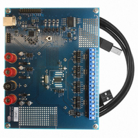
BOARD EVAL FOR CS5467 ADC
Manufacturer
Cirrus Logic Inc
Type
A/Dr
Specifications of CDB5467U
Main Purpose
Power Management, Energy/Power Meter
Embedded
Yes, MCU, 8-Bit
Utilized Ic / Part
CS5467
Primary Attributes
Watt-Hour Meter
Secondary Attributes
Graphical User Interface, SPI™ & USB Interfaces
Product
Data Conversion Development Tools
Maximum Clock Frequency
4 MHz
Interface Type
USB
Supply Voltage (max)
5 V
Supply Voltage (min)
3.3 V
For Use With/related Products
CS5467
Lead Free Status / RoHS Status
Contains lead / RoHS non-compliant
Lead Free Status / RoHS Status
Lead free / RoHS Compliant, Contains lead / RoHS non-compliant
Other names
598-1555
CDB-5467U
CDB-5467U


2.5.1
In the offset and gain register boxes, the offset and gain registers for all channels are displayed in hexa-
decimal and decimal. These registers can be modified directly by typing the desired value in the hexadec-
imal display boxes. There are three types of offset registers: DC offset, AC offset and power offset. The
AC offset registers only affect the RMS register values. The power offset registers only affect the active
power register values. The DC/AC/power offset register is a two's complement number whose value rang-
es from -1 to +1. The gain register value ranges from 0 to 4.
2.5.2
AC/DC offset and gain calibrations can be performed on both the voltage and current channels of the
CS5467. It is generally a good idea to software-reset the CS5467 before running calibrations, because
the initial values in the calibration registers will affect the results of the calibration. A software reset will
reset these registers back to the default values of zero offset and unity gain. AC/DC offset calibration
should be performed before gain calibration to ensure accurate results.
2.5.2.1
2.5.2.2
The Calibration window also contains the Power Offset Register1 / 2 display and adjustment. The user
can read and write the values in the power offset registers (P1off / P2off).
DS714DB1
1. Ground the channel(s) you want to calibrate directly at the channel header(s), J11 and J7 for voltage chan-
2. Press the corresponding AC or DC offset calibrate button (Cal V, Cal I, or Calibrate All Channels) beside or
3. The offset register value(s) will automatically update when the calibration is completed.
1. Attach an AC or DC calibration signal to the screw-type terminals, and make sure the corresponding chan-
2. Press the corresponding AC or DC gain calibrate button (Cal V, Cal I, or Calibrate All Channels) beside or
3. The gain register value(s) will automatically update when the calibration is completed.
nel 2, J17 and J22 for voltage channel 1, J24 and J26 for current channel 1, and J20 and J19 for current
channel 2. The channel(s) could also be grounded directly at the screw-type terminals.
below the offset register boxes.
nel headers (J11, J7, J17, J22, J24, J26, J20 and J19) are set to the input position.
below the gain register boxes.
Offset / Gain Register
Performing Calibrations
Offset Calibrations
Gain Calibrations
CDB5467U
15
Related parts for CDB5467U
Image
Part Number
Description
Manufacturer
Datasheet
Request
R

Part Number:
Description:
Development Kit
Manufacturer:
Cirrus Logic Inc
Datasheet:
Part Number:
Description:
Development Kit
Manufacturer:
Cirrus Logic Inc
Datasheet:


Part Number:
Description:
High-efficiency PFC + Fluorescent Lamp Driver Reference Design
Manufacturer:
Cirrus Logic Inc
Datasheet:
Part Number:
Description:
Development Kit
Manufacturer:
Cirrus Logic Inc
Datasheet:
Part Number:
Description:
Development Kit
Manufacturer:
Cirrus Logic Inc
Datasheet:

Part Number:
Description:
Development Kit
Manufacturer:
Cirrus Logic Inc
Datasheet:
Part Number:
Description:
Development Kit
Manufacturer:
Cirrus Logic Inc
Datasheet:
Part Number:
Description:
Development Kit
Manufacturer:
Cirrus Logic Inc
Datasheet:
Part Number:
Description:
Development Kit
Manufacturer:
Cirrus Logic Inc
Datasheet:

Part Number:
Description:
EVALUATION BOARD FOR CS8427
Manufacturer:
Cirrus Logic Inc
Datasheet:

Part Number:
Description:
BOARD EVAL FOR CS8416 RCVR
Manufacturer:
Cirrus Logic Inc
Datasheet:

Part Number:
Description:
EVALUATION BOARD FOR CS8420
Manufacturer:
Cirrus Logic Inc
Datasheet:

Part Number:
Description:
KIT DEVELOPMENT EP9315 ARM9
Manufacturer:
Cirrus Logic Inc
Datasheet:

Part Number:
Description:
KIT DEVELOPMENT EP9302 ARM9
Manufacturer:
Cirrus Logic Inc
Datasheet: