CDB42L51 Cirrus Logic Inc, CDB42L51 Datasheet - Page 28
CDB42L51
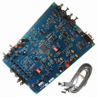
Manufacturer Part Number
CDB42L51
Description
BOARD EVAL FOR CS42L51 CODEC
Manufacturer
Cirrus Logic Inc
Specifications of CDB42L51
Main Purpose
Audio, CODEC
Embedded
Yes, Other
Utilized Ic / Part
CS42L51, CS8406, CS8415
Primary Attributes
Stereo, Digital Audio Transmitter and Receiver
Secondary Attributes
Graphic User Interface, S/PDIF Interface
Description/function
Audio CODECs
Operating Supply Voltage
5 V
Product
Audio Modules
For Use With/related Products
CS42L51
Lead Free Status / RoHS Status
Contains lead / RoHS non-compliant
Lead Free Status / RoHS Status
Lead free / RoHS Compliant, Contains lead / RoHS non-compliant
Other names
598-1005


28
4.3
4.3.1
DIGMIX
MUX
MUX
AINxA and AINxB are the analog inputs, internally biased to VQ, that accepts line-level and MIC-level sig-
nals, allowing various gain and signal adjustments for each channel.
Analog Inputs
Digital Code, Offset & DC Measurement
The ADC output data is in two’s complement binary format. For inputs above positive full scale or below
negative full scale, the ADC will output 7FFFFFH or 800000H, respectively and cause the ADC overflow
bit to be set to a ‘1’.
Given the two’s complement format, low-level signals may cause the MSB of the serial data to periodically
toggle between ‘1’ and ‘0’, possibly introducing noise into the system as the bit switches back and forth.
To prevent this phenomena, a constant DC offset is added to the serial data bringing the low-level signal
just above the point at which the MSB would normally toggle, thus reducing the noise introduced. Note
that this offset is not removed (refer to
and/or
The CODEC may be used to measure DC voltages by disabling the high-pass filter for the designated
channel. DC levels are measured relative to VQ and will be decoded as positive two’s complement binary
numbers above VQ and negative two’s complement binary numbers below VQ.
Software
Controls:
“Analog Input Characteristics (Automotive - DNZ)” on page 14
MICMIX
MUX
MUX
“Status (Address 20h) (Read Only)” on page
Σ
ADCA_HPF FREEZE
ADCA_HPF ENABLE
ADCB_HPF FREEZE
ADCB_HPF ENABLE
ALC_ARATE[5:0]
ALC_RRATE[5:0]
ALCA_SRDIS
ALCA_ZCDIS
ALCB_SRDIS
ALCB_ZCDIS
MAX[2:0]
MIN[2:0]
ALC_ENB
ALC_ENA
Figure 8. Analog Input Architecture
ADCA_DBOOST
ALC
TO SIGNAL PROCESSING
ENGINE (SPE)
FROM SIGNAL
PROCESSING ENGINE
(SPE)
ADCB_DBOOST
+20dB
+20dB
Digital
Digital
Boost
Boost
“Analog Input Characteristics (Commercial - CNZ)” on page 13
ADCA_ATT[7:0]
ADCB_ATT[7:0]
ADCB_MUTE
1dB steps
0/-96dB
SOFTB
ADCA_MUTE
1dB steps
SOFTA
0/-96dB
Attenuator
Attenuator
Noise Gate
73,
PDN_ADCA
“ADC Control (Address 06h)” on page
PDN_ADCB
NG_ALL
NG_EN
THRESH[3:0]
NGDELAY[1:0]
Oversampling
Oversampling
INV_ADCA
INV_ADCB
Multibit
Multibit
ADC
ADC
for the specified offset level).
PGA
PGA
PDN_PGAB
AINB_MUX[1:0]
AINA_MUX[1:0]
PGAA_VOL[5:0]
ADC_SNGVOL
SOFTA
ZCROSSA
MICBIAS_LVL[1:0]
PDN_MICBIAS
0.5dB steps
0.5dB steps
PGAB_VOL[5:0]
ADC_SNGVOL
SOFTB
ZCROSSB
PDN_PGAA
+12/-3dB
+12/-3dB
MUX
MUX
MICBIAS
32 dB
+16/
32 dB
+16/
MICBIAS_SEL
PDN_MICA
MICA_BOOST
PDN_MICB
MICB_BOOST
CS42L51
AIN1A
AIN2A
AIN3A/ MICIN1
AIN1B
AIN2B/MICBIAS
AIN3B/ MICIN2/
MICBIAS
54.
DS679F1
Related parts for CDB42L51
Image
Part Number
Description
Manufacturer
Datasheet
Request
R

Part Number:
Description:
Development Kit
Manufacturer:
Cirrus Logic Inc
Datasheet:
Part Number:
Description:
Development Kit
Manufacturer:
Cirrus Logic Inc
Datasheet:


Part Number:
Description:
High-efficiency PFC + Fluorescent Lamp Driver Reference Design
Manufacturer:
Cirrus Logic Inc
Datasheet:
Part Number:
Description:
Development Kit
Manufacturer:
Cirrus Logic Inc
Datasheet:
Part Number:
Description:
Development Kit
Manufacturer:
Cirrus Logic Inc
Datasheet:

Part Number:
Description:
Development Kit
Manufacturer:
Cirrus Logic Inc
Datasheet:
Part Number:
Description:
Development Kit
Manufacturer:
Cirrus Logic Inc
Datasheet:
Part Number:
Description:
Development Kit
Manufacturer:
Cirrus Logic Inc
Datasheet:
Part Number:
Description:
Development Kit
Manufacturer:
Cirrus Logic Inc
Datasheet:

Part Number:
Description:
EVALUATION BOARD FOR CS8427
Manufacturer:
Cirrus Logic Inc
Datasheet:

Part Number:
Description:
BOARD EVAL FOR CS8416 RCVR
Manufacturer:
Cirrus Logic Inc
Datasheet:

Part Number:
Description:
EVALUATION BOARD FOR CS8420
Manufacturer:
Cirrus Logic Inc
Datasheet:

Part Number:
Description:
KIT DEVELOPMENT EP9315 ARM9
Manufacturer:
Cirrus Logic Inc
Datasheet:

Part Number:
Description:
KIT DEVELOPMENT EP9302 ARM9
Manufacturer:
Cirrus Logic Inc
Datasheet: