STEVAL-ISB001V1 STMicroelectronics, STEVAL-ISB001V1 Datasheet - Page 14
STEVAL-ISB001V1
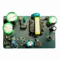
Manufacturer Part Number
STEVAL-ISB001V1
Description
BATTERY CHARGER CELL PHONE
Manufacturer
STMicroelectronics
Type
Battery Managementr
Specifications of STEVAL-ISB001V1
Main Purpose
Power Management, Battery Charger
Embedded
No
Utilized Ic / Part
STD1LNK60Z
Primary Attributes
1 Cell, 4.7V @ 400mA Out, CV/CC, 85 ~ 265VAC Input, 1.9W
Secondary Attributes
>65% Efficient, 51 ~ 91mW Standby Input Power
Input Voltage
85 V to 265 V
Output Voltage
5 V
Product
Power Management Modules
Silicon Manufacturer
ST Micro
Silicon Core Number
STD1LNK60Z-1
Kit Application Type
Power Management - Battery
Application Sub Type
Battery Charger
Kit Contents
Board
Rohs Compliant
No
Lead Free Status / RoHS Status
Lead free / RoHS Compliant
For Use With/related Products
STD1LNK60Z
Other names
497-5682
Available stocks
Company
Part Number
Manufacturer
Quantity
Price
Company:

Part Number:
STEVAL-ISB001V1
Manufacturer:
STMicroelectronics
Quantity:
1


2 STD1LNK60Z-based RCC Control Circuit Components
2.4
2.4.1
2.4.2
2.4.3
14/26
R7 Sense Resistor
Minimum Power Dissipation
Sense resistor R7 is used to detect primary peak current. It is limited by its maximum power
dissipation, which is set to 0.1% of the maximum power. The minimum power dissipation is
expressed as
Maximum Power Dissipation
If R
Sense Resistors and the Power Margin
Two resistors (6.8 , and 6.8 , respectively) are placed in parallel to produce the required
sense resistor value and still have enough power margin.
Ramp-up voltage (via R
output voltage and current regulation (see
Note: The R9 value should be much greater than the R7 value. The minimum primary current,
I
I
The cathode current, I
current of optocoupler PC817 is 50mA. In order to decrease quiescent power dissipation, the
maximum operation diode current, I
The Current Transfer Ratio (CTR) of PC817 is about 1:0 at the stead state. As a result, the
maximum operation transistor current I
neglected.
At minimum load,
At maximum load,
where,
V
reaches this value, MOSFET Q1 is turned off.
For the purposes of this application design:
R
C
ppk
ppk
Qbe
9
6
= 360 , and
= 2.2nF; the role of C
7
, and the maximum current, I
and the minimum I
is set to 3.4 , its maximum power dissipation is expressed as
= Cut off voltage; when the voltage between the base and the emitter of transistor Q2
R
7
I
F m in
R
7
P
I
+
ppk
R
R7 max
7
R
k
2
, of TL431 is limited to 1mA< I
+
7
7
0.01 V
----------------------------------------------- -
are in a stead state at the maximum load.
6
+
x I
R
is to accelerate the MOSFET’s turning OFF.
R
7
ppk
9
=
+
I
I
), when added to the DC voltage [(I
prms
I
R
e max
prms
2
o
9
, are in a stead state at the minimum load, while the maximum
I
o max
I
2
F
e m in
2
, of PC817 can be set to 10mA.
R
e
7
of PC817 is also set to 10mA. Initially the effect of I
R
=
=
7
Figure 4
0.01
-------------------------------------- -
0.062
R
+
0.7
7
R
I
ppk
9
2
I
5
0.062
e ma x
+
).
3.4
R
k
0.48
9
<100mA, and the maximum diode
I
2
e min
=
0.013W
=
R
AN2228 - APPLICATION NOTE
8.9
9
I
e m ax
V
1
Q be
+I
e
)(R
V
Q be
7
+R
9
)] achieves good
1
is
Related parts for STEVAL-ISB001V1
Image
Part Number
Description
Manufacturer
Datasheet
Request
R

Part Number:
Description:
BOARD RGB CTR ST7,STP08C596MTR
Manufacturer:
STMicroelectronics
Datasheet:

Part Number:
Description:
Power Management IC Development Tools Full Speed USB to RS232 Bridge Demo
Manufacturer:
STMicroelectronics
Datasheet:
Part Number:
Description:
Power Management IC Development Tools 2.5W solar eval BRD USB SPV1040 LD39050
Manufacturer:
STMicroelectronics
Datasheet:

Part Number:
Description:
BOARD EVAL FOR MEMS SENSORS
Manufacturer:
STMicroelectronics
Datasheet:

Part Number:
Description:
KIT DEV STARTER ST10F276Z5
Manufacturer:
STMicroelectronics
Datasheet:

Part Number:
Description:
BOARD EVAL HDMI $ VIDEO SWITCH
Manufacturer:
STMicroelectronics
Datasheet:

Part Number:
Description:
BOARD DEMO ACCELEROMETER DIL24
Manufacturer:
STMicroelectronics
Datasheet:

Part Number:
Description:
BOARD STLM75/STDS75/ST72F651
Manufacturer:
STMicroelectronics
Datasheet:

Part Number:
Description:
EVAL BOARD 3AXIS MEMS ACCELLRMTR
Manufacturer:
STMicroelectronics
Datasheet:

Part Number:
Description:
BOARD EVAL 8BIT MICRO + TDE1708
Manufacturer:
STMicroelectronics
Datasheet:
Part Number:
Description:
STMicroelectronics [RIPPLE-CARRY BINARY COUNTER/DIVIDERS]
Manufacturer:
STMicroelectronics
Datasheet:
Part Number:
Description:
STMicroelectronics [LIQUID-CRYSTAL DISPLAY DRIVERS]
Manufacturer:
STMicroelectronics
Datasheet:
Part Number:
Description:
BOARD EVAL FOR MEMS SENSORS
Manufacturer:
STMicroelectronics
Datasheet: