NCP345EVB ON Semiconductor, NCP345EVB Datasheet - Page 3
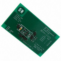
NCP345EVB
Manufacturer Part Number
NCP345EVB
Description
EVAL BOARD FOR NCP345
Manufacturer
ON Semiconductor
Specifications of NCP345EVB
Design Resources
NCP345 Demo Board BOM NCP345EVB Gerber Files NCP345/6 EVB Schematic
Main Purpose
Overvoltage Protection
Embedded
No
Utilized Ic / Part
NCP345
Lead Free Status / RoHS Status
Lead free / RoHS Compliant
Secondary Attributes
-
Primary Attributes
-
Lead Free Status / Rohs Status
Lead free / RoHS Compliant
For Use With/related Products
NCP345
Other names
NCP345EVBOS


Stresses exceeding Maximum Ratings may damage the device. Maximum Ratings are stress ratings only. Functional operation above the
Recommended Operating Conditions is not implied. Extended exposure to stresses above the Recommended Operating Conditions may affect
device reliability.
{ Human body model (HBM): MIL STD 883C Method 3015−7, (R = 1500 ohms, C = 100 pf, F = 3 pulses delay 1 s).
*Turn ON Delay is guaranteed by design.
ABSOLUTE MAXIMUM RATINGS
ELECTRICAL CHARACTERISTICS
(For typical values T
OUT voltage to GND
Input and CNTRL pin voltage to GND
V
Maximum Power Dissipation at T
Thermal Resistance Junction to Air
Junction Temperature
Operating Ambient Temperature
V
Storage Temperature Range
ESD performance (HBM){
V
Supply Current (I
Input Threshold
Input Hysteresis (V
Input Impedance (Input = V
CNTRL Voltage High
CNTRL Voltage Low
CNTRL Current High (V
CNTRL Current Low (V
Undervoltage Lockout (V
Output Sink Current (V
Output Voltage High (V
Output Voltage High (V
Output Voltage High (V
Output Voltage Low
Turn ON Delay − Input (V
Turn OFF Delay − Input (V
Turn ON Delay − CNTRL (CNTRL step down signal from 2.0 to 0.5 V;
Turn OFF Delay − CNTRL (CNTRL step up signal from 0.5 to 2.0 V;
(V
(Input < 6.5 V; I
signal from 8.0 to 6.0 V; measured to 50% point of OUT)*
from 6.0 to 8.0 V; C
measured to 50% point of OUT)*
C
CC
CNTRL
CC
L
Input
= 12 nF Output > V
Maximum Range
Operating Voltage Range
Operating Voltage
connected to V
Sink
CC
A
Input
+ I
= 0 mA; V
L
= 25°C, for min/max values T
= 12 nF Output > V
CC
Input
CC
CC
CC
CC
il
CC
connected to V
ih
= 0.5 V)
CC
Input
; V
= 5.0 V)
< V
−1.0 V)
= V
= V
= V
Input
; V
Th
Characteristic
decreasing)
Rating
Input
)
Th
CC
in
in
in
connected to V
CC
connected to V
, V
= 8.0 V; I
= 8.0 V; I
= 8.0 V; I
A
= 6.0 V Steady State)
increasing)
= 6.0 V, CNTRL = 0 V)
OUT
= 85°C
(T
CC
= 1.0 V)
A
Source
Source
Source
; V
CC
= 25°C unless otherwise noted.)
−1.0 V)
Input
CC
CC
= 10 mA)
= 0.25 mA)
= 0 mA)
; V
; V
decreasing)
A
Input
Input
= −40°C to +85°C, V
step down
http://onsemi.com
step up signal
NCP345
3
Pin
all
1
4
3
5
−
−
−
−
3
−
CC
Symbol
V
T
T
T
T
V
V
OFF CT
CC(opt)
= 6.0 V, unless otherwise noted.)
OFF IN
I
ON CT
V
V
ON IN
R
V
Sink
V
Hyst
V
I
Lock
I
−
ih
Th
oh
il
ol
in
ih
il
V
Symbol
V
CC(max)
V
R
CNTRL
T
V
P
input
T
T
Pin
qJA
−
stg
−
4,5
O
A
D
J
5
4
4
4
3
3
3
3
3
1
1
1
1
1
1
1
V
V
V
CC
CC
CC
6.65
Min
3.0
1.5
2.5
50
70
10
−0.25
−
−
−
−
−
−
−
−
−
−1.0
−0.1
−0.3
−0.3
−0.3
−0.3
Min
−40
−65
2.5
−
−
−
0
0.75
6.85
Typ
100
150
4.8
2.8
0.5
1.0
95
10
33
−
−
−
−
−
−
−
0.216
Max
300
150
150
5.0
30
30
13
30
85
−
Max
7.08
200
200
1.0
0.5
3.0
0.1
1.0
2.0
25
20
50
10
10
−
−
−
−
°C/W
Unit
kV
°C
°C
°C
W
V
V
V
V
msec
msec
msec
msec
Unit
mA
mV
kW
mA
mA
mA
V
V
V
V
V
V
V
Related parts for NCP345EVB
Image
Part Number
Description
Manufacturer
Datasheet
Request
R

Part Number:
Description:
ON Semiconductor [VOLTAGE REGULATOR]
Manufacturer:
ON Semiconductor
Datasheet:
Part Number:
Description:
357-036-542-201 CARDEDGE 36POS DL .156 BLK LOPRO
Manufacturer:
ON Semiconductor
Datasheet:
Part Number:
Description:
357-036-542-201 CARDEDGE 36POS DL .156 BLK LOPRO
Manufacturer:
ON Semiconductor
Datasheet:
Part Number:
Description:
357-036-542-201 CARDEDGE 36POS DL .156 BLK LOPRO
Manufacturer:
ON Semiconductor
Datasheet:
Part Number:
Description:
357-036-542-201 CARDEDGE 36POS DL .156 BLK LOPRO
Manufacturer:
ON Semiconductor
Datasheet:
Part Number:
Description:
357-036-542-201 CARDEDGE 36POS DL .156 BLK LOPRO
Manufacturer:
ON Semiconductor
Datasheet:
Part Number:
Description:
357-036-542-201 CARDEDGE 36POS DL .156 BLK LOPRO
Manufacturer:
ON Semiconductor
Datasheet:
Part Number:
Description:
357-036-542-201 CARDEDGE 36POS DL .156 BLK LOPRO
Manufacturer:
ON Semiconductor
Datasheet:
Part Number:
Description:
357-036-542-201 CARDEDGE 36POS DL .156 BLK LOPRO
Manufacturer:
ON Semiconductor
Datasheet:
Part Number:
Description:
357-036-542-201 CARDEDGE 36POS DL .156 BLK LOPRO
Manufacturer:
ON Semiconductor
Datasheet:
Part Number:
Description:
357-036-542-201 CARDEDGE 36POS DL .156 BLK LOPRO
Manufacturer:
ON Semiconductor
Datasheet:
Part Number:
Description:
Manufacturer:
ON Semiconductor
Datasheet:
Part Number:
Description:
Manufacturer:
ON Semiconductor
Datasheet: