NCP345EVB ON Semiconductor, NCP345EVB Datasheet - Page 6
NCP345EVB
Manufacturer Part Number
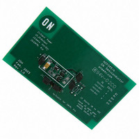
NCP345EVB
Description
EVAL BOARD FOR NCP345
Manufacturer
ON Semiconductor
Specifications of NCP345EVB
Design Resources
NCP345 Demo Board BOM NCP345EVB Gerber Files NCP345/6 EVB Schematic
Main Purpose
Overvoltage Protection
Embedded
No
Utilized Ic / Part
NCP345
Lead Free Status / RoHS Status
Lead free / RoHS Compliant
Secondary Attributes
-
Primary Attributes
-
Lead Free Status / Rohs Status
Lead free / RoHS Compliant
For Use With/related Products
NCP345
Other names
NCP345EVBOS


Normal Operation
adapter provides power to the protection system so the
circuitry is only active when the adapter is connected. The
OVP monitors the voltage from the charger and if the
voltage exceeds a nominal voltage of 6.85 V, the OUT signal
drives the gate of the MOSFET to within 1.0 V of V
turning off the FET and disconnecting the source from the
load. The nominal time it takes to drive the gate to this state
is 400 nsec (1.0 usec maximum for gate capacitance of
< 12 nF). Typical turn off performance using the CNTRL
input can be seen in Figure 6. The CNTRL input can also be
used to interrupt charging and allow the microcontroller to
measure the cell voltage under a normal condition to get a
more accurate measure of the battery voltage. Once the over
voltage is removed, the NCP345 will turn on the MOSFET.
The turn on circuitry is designed to turn on the MOSFET
more gradually to limit the in−rush current. Typical turn−on
Figure 1 illustrates a typical configuration. The external
CC
http://onsemi.com
, thus
NCP345
6
performance is illustrated using the MGSF3441 in Figure 7.
This characteristic is a function of the threshold of the
MOSFET and will vary depending on the device
characteristics such as the gate capacitance.
which disables the gate driver circuit until the UVLO senses
that the V
released the gate driver circuit, the OUT signal will stay high
until the voltage on the IN is sensed. If the input voltage to
IN is less than 6.85 V nominal, then the OUT signal will be
driven LOW and the FET will be turned on so the source can
be connected to the load.
gate of the FET to a HIGH state.
•
•
•
The OVP has an under voltage lockout (UVLO) circuit
There are three events that will cause the OVP to drive the
Voltage on V
Voltage on IN rises above 6.85 V (nominal)
CNTRL input is driven to a logic High
CC
voltage is above 2.6 V. Once the UVLO has
CC
falls below the UVLO threshold
Related parts for NCP345EVB
Image
Part Number
Description
Manufacturer
Datasheet
Request
R

Part Number:
Description:
ON Semiconductor [VOLTAGE REGULATOR]
Manufacturer:
ON Semiconductor
Datasheet:
Part Number:
Description:
357-036-542-201 CARDEDGE 36POS DL .156 BLK LOPRO
Manufacturer:
ON Semiconductor
Datasheet:
Part Number:
Description:
357-036-542-201 CARDEDGE 36POS DL .156 BLK LOPRO
Manufacturer:
ON Semiconductor
Datasheet:
Part Number:
Description:
357-036-542-201 CARDEDGE 36POS DL .156 BLK LOPRO
Manufacturer:
ON Semiconductor
Datasheet:
Part Number:
Description:
357-036-542-201 CARDEDGE 36POS DL .156 BLK LOPRO
Manufacturer:
ON Semiconductor
Datasheet:
Part Number:
Description:
357-036-542-201 CARDEDGE 36POS DL .156 BLK LOPRO
Manufacturer:
ON Semiconductor
Datasheet:
Part Number:
Description:
357-036-542-201 CARDEDGE 36POS DL .156 BLK LOPRO
Manufacturer:
ON Semiconductor
Datasheet:
Part Number:
Description:
357-036-542-201 CARDEDGE 36POS DL .156 BLK LOPRO
Manufacturer:
ON Semiconductor
Datasheet:
Part Number:
Description:
357-036-542-201 CARDEDGE 36POS DL .156 BLK LOPRO
Manufacturer:
ON Semiconductor
Datasheet:
Part Number:
Description:
357-036-542-201 CARDEDGE 36POS DL .156 BLK LOPRO
Manufacturer:
ON Semiconductor
Datasheet:
Part Number:
Description:
357-036-542-201 CARDEDGE 36POS DL .156 BLK LOPRO
Manufacturer:
ON Semiconductor
Datasheet:
Part Number:
Description:
Manufacturer:
ON Semiconductor
Datasheet:
Part Number:
Description:
Manufacturer:
ON Semiconductor
Datasheet: