NCP345EVB ON Semiconductor, NCP345EVB Datasheet - Page 7
NCP345EVB
Manufacturer Part Number
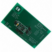
NCP345EVB
Description
EVAL BOARD FOR NCP345
Manufacturer
ON Semiconductor
Specifications of NCP345EVB
Design Resources
NCP345 Demo Board BOM NCP345EVB Gerber Files NCP345/6 EVB Schematic
Main Purpose
Overvoltage Protection
Embedded
No
Utilized Ic / Part
NCP345
Lead Free Status / RoHS Status
Lead free / RoHS Compliant
Secondary Attributes
-
Primary Attributes
-
Lead Free Status / Rohs Status
Lead free / RoHS Compliant
For Use With/related Products
NCP345
Other names
NCP345EVBOS


0.05 (0.002)
S
H
1
D
5
L
A
2
G
*For additional information on our Pb−Free strategy and soldering
4
3
details, please download the ON Semiconductor Soldering and
Mounting Techniques Reference Manual, SOLDERRM/D.
C
B
0.039
1.0
0.037
PACKAGE DIMENSIONS
0.95
SOLDERING FOOTPRINT*
http://onsemi.com
THIN SOT−23−5
CASE 483−02
K
SN SUFFIX
ISSUE E
NCP345
0.074
1.9
7
J
0.028
0.7
M
SCALE 10:1
0.094
2.4
NOTES:
1. DIMENSIONING AND TOLERANCING PER
2. CONTROLLING DIMENSION: MILLIMETER.
3. MAXIMUM LEAD THICKNESS INCLUDES
4. A AND B DIMENSIONS DO NOT INCLUDE
ANSI Y14.5M, 1982.
LEAD FINISH THICKNESS. MINIMUM LEAD
THICKNESS IS THE MINIMUM THICKNESS
OF BASE MATERIAL.
MOLD FLASH, PROTRUSIONS, OR GATE
BURRS.
DIM
A
B
C
D
G
H
K
M
J
L
S
inches
mm
0.013
MILLIMETERS
MIN
2.90
1.30
0.90
0.25
0.85
0.10
0.20
1.25
2.50
0
_
0.100
MAX
3.10
1.70
1.10
0.50
1.05
0.26
0.60
1.55
10
3.00
_
0.0512
0.0354
0.0098
0.0335
0.0005
0.0040
0.0079
0.0493
0.0985
0.1142
MIN
0
INCHES
_
0.1220
0.0669
0.0433
0.0197
0.0413
0.0040
0.0102
0.0236
0.0610
0.1181
MAX
10
_
Related parts for NCP345EVB
Image
Part Number
Description
Manufacturer
Datasheet
Request
R

Part Number:
Description:
ON Semiconductor [VOLTAGE REGULATOR]
Manufacturer:
ON Semiconductor
Datasheet:
Part Number:
Description:
357-036-542-201 CARDEDGE 36POS DL .156 BLK LOPRO
Manufacturer:
ON Semiconductor
Datasheet:
Part Number:
Description:
357-036-542-201 CARDEDGE 36POS DL .156 BLK LOPRO
Manufacturer:
ON Semiconductor
Datasheet:
Part Number:
Description:
357-036-542-201 CARDEDGE 36POS DL .156 BLK LOPRO
Manufacturer:
ON Semiconductor
Datasheet:
Part Number:
Description:
357-036-542-201 CARDEDGE 36POS DL .156 BLK LOPRO
Manufacturer:
ON Semiconductor
Datasheet:
Part Number:
Description:
357-036-542-201 CARDEDGE 36POS DL .156 BLK LOPRO
Manufacturer:
ON Semiconductor
Datasheet:
Part Number:
Description:
357-036-542-201 CARDEDGE 36POS DL .156 BLK LOPRO
Manufacturer:
ON Semiconductor
Datasheet:
Part Number:
Description:
357-036-542-201 CARDEDGE 36POS DL .156 BLK LOPRO
Manufacturer:
ON Semiconductor
Datasheet:
Part Number:
Description:
357-036-542-201 CARDEDGE 36POS DL .156 BLK LOPRO
Manufacturer:
ON Semiconductor
Datasheet:
Part Number:
Description:
357-036-542-201 CARDEDGE 36POS DL .156 BLK LOPRO
Manufacturer:
ON Semiconductor
Datasheet:
Part Number:
Description:
357-036-542-201 CARDEDGE 36POS DL .156 BLK LOPRO
Manufacturer:
ON Semiconductor
Datasheet:
Part Number:
Description:
Manufacturer:
ON Semiconductor
Datasheet:
Part Number:
Description:
Manufacturer:
ON Semiconductor
Datasheet: