MCP355XDV-MS1 Microchip Technology, MCP355XDV-MS1 Datasheet - Page 14
MCP355XDV-MS1
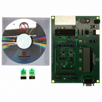
Manufacturer Part Number
MCP355XDV-MS1
Description
BOARD DEV SENSOR APP MCP355X
Manufacturer
Microchip Technology
Datasheets
1.MCP3553-ESN.pdf
(36 pages)
2.MCP355XDV-MS1.pdf
(36 pages)
3.MCP3551DM-PCTL.pdf
(30 pages)
Specifications of MCP355XDV-MS1
Number Of Adc's
1
Number Of Bits
22
Data Interface
Serial
Inputs Per Adc
1 Differential
Input Range
±0.3 V
Voltage Supply Source
Single Supply
Operating Temperature
-40°C ~ 125°C
Utilized Ic / Part
MCP355x
Processor To Be Evaluated
MCP355x
Interface Type
RS-232, USB
Lead Free Status / RoHS Status
Not applicable / Not applicable
Lead Free Status / RoHS Status
Lead free / RoHS Compliant, Not applicable / Not applicable
Available stocks
Company
Part Number
Manufacturer
Quantity
Price
Company:

Part Number:
MCP355XDV-MS1
Manufacturer:
MICROCHIP
Quantity:
12 000


MCP355X Sensor Application Developer’s Board User’s Guide
DS51609A-page 10
FIGURE 2-4:
cancellation.
2.3.1
The analog switches are used with the amplifier to swap the sources driving the load
cell, effectively cancelling any offset or offset drift. One conversion is performed with
the load cell driven “normally” and a second while it is driven in an “inverted”
configuration. The result of the second conversion is inverted and added to the result
from the first and an average of the two is computed (computing the average is a simple
shift operation for the microcontroller). This technique effectively cancels the offset of
the amplifiers as well as the ADC. An offset residue will exist if the any of the offsets
change between conversions. This is unlikely to happen unless the temperature
changes rapidly after the first conversion. The offset of the sensor is not affected by this
technique.
The firmware included with this developer’s board performs this process when
“Channel 1” is selected using the push button switches.
This process is described here:
1. Stop the output drive by configuring the outputs of the PICmicro MCU that drive
2. Control the analog switches and switch the ground of the MCP3551 to the
3. Start the output drive by configuring the output of the PICmicro MCU that drives
4. Perform a conversion and save the result.
5. Stop the output drive by configuring both outputs of the PICmicro MCU that drive
6. Control the analog switches and switch the ground of the MCP3551 to the “top”
7. Start the output drive by configuring the output of the PICmicro MCU that drives
8. Perform a conversion, invert the result, add to the first conversion, divide by two,
SPI
the load cell as low.
“bottom” of the load cell and the reference of the MCP3551 to the “top” of the load
cell.
the “top” of the load cell as high.
the load cell as low.
of the load cell and the reference of the MCP3551 to the “bottom” of the load cell.
the “bottom” of the load cell as high.
and save the result as the actual reading.
Switch Control From PIC16F877
Channel 1 Analog Switches and Offset Drift Cancellation
V
MCP3551
REF
V
SS
U5
Channel 1 Differential Gain Circuit with analog switch offset
V
V
IN+
IN-
MCP6XX Socket U9
Analog Switch
Analog Switch
U7
R
F
+
+
-
-
U8
R
G
© 2006 Microchip Technology Inc.
P6
-SENSE
-IN
-OUT
+OUT
+IN
+SENSE
Related parts for MCP355XDV-MS1
Image
Part Number
Description
Manufacturer
Datasheet
Request
R

Part Number:
Description:
Manufacturer:
Microchip Technology Inc.
Datasheet:
Part Number:
Description:
Manufacturer:
Microchip Technology Inc.
Datasheet:
Part Number:
Description:
Manufacturer:
Microchip Technology Inc.
Datasheet:
Part Number:
Description:
Manufacturer:
Microchip Technology Inc.
Datasheet:
Part Number:
Description:
Manufacturer:
Microchip Technology Inc.
Datasheet:
Part Number:
Description:
Manufacturer:
Microchip Technology Inc.
Datasheet:
Part Number:
Description:
Manufacturer:
Microchip Technology Inc.
Datasheet:
Part Number:
Description:
Manufacturer:
Microchip Technology Inc.
Datasheet: