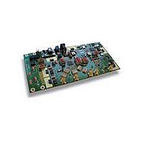
ADC1415S125/DB,598 NXP Semiconductors, ADC1415S125/DB,598 Datasheet - Page 15

ADC1415S125/DB,598
Manufacturer Part Number
ADC1415S125/DB,598
Description
BOARD DEMO FOR ADC1415S125
Manufacturer
NXP Semiconductors
Type
A/Dr
Datasheets
1.ADC1415S125HNC15.pdf
(42 pages)
2.HSDC-ACC01DB.pdf
(32 pages)
3.ADC1415S125DB598.pdf
(2 pages)
Specifications of ADC1415S125/DB,598
Number Of Adc's
1
Number Of Bits
14
Sampling Rate (per Second)
125M
Data Interface
Serial, SPI™
Inputs Per Adc
1 Differential
Input Range
1 ~ 2 Vpp
Power (typ) @ Conditions
840mW @ 125Msps
Voltage Supply Source
Single Supply
Operating Temperature
-40°C ~ 85°C
Utilized Ic / Part
ADC1415S125
Product
Data Conversion Development Tools
Conversion Rate
125 MSPS
Resolution
14 bit
Interface Type
SMA
For Use With/related Products
ADC1415S125
Lead Free Status / RoHS Status
Lead free / RoHS Compliant
Lead Free Status / RoHS Status
Lead free / RoHS Compliant, Lead free / RoHS Compliant
Other names
568-5094
NXP Semiconductors
ADC1415S_SER
Product data sheet
10.3 SPI timings
Table 9.
[1]
Symbol
t
t
t
t
t
f
w(SCLK)
w(SCLKH)
w(SCLKL)
su
h
clk(max)
Fig 6.
Typical values measured at V
minimum and maximum values are across the full temperature range T
V
DDA
= 3 V, V
SPI timing
SCLK
SPI timings characteristics
SDIO
Parameter
SCLK pulse width
SCLK HIGH pulse width
SCLK LOW pulse width
set-up time
hold time
maximum clock frequency
CS
DDO
All information provided in this document is subject to legal disclaimers.
Single 14-bit ADC; input buffer; CMOS or LVDS DDR digital outputs
= 1.8 V
t
su
Rev. 4 — 17 December 2010
R/W
DDA(3V)
W1
t
h
t
su
= 3 V, V
W0
t
w(SCLK)
[1]
DDO
A12
Conditions
data to SCLK HIGH
CS to SCLK HIGH
data to SCLK HIGH
CS to SCLK HIGH
= 1.8 V, V
A11
t
w(SCLKL)
DDA(5V)
ADC1415S series
t
w(SCLKH)
D2
= 5 V, T
amb
-
-
-
-
Min
-
-
-
-
D1
amb
= −40 °C to +85 °C at
= 25 °C and C
Typ
40
16
16
5
5
2
2
25
D0
© NXP B.V. 2010. All rights reserved.
t
h
005aaa065
Max
-
-
-
-
-
-
-
-
L
= 5 pF;
15 of 42
Unit
ns
ns
ns
ns
ns
ns
ns
MHz


