ADC1415S125/DB,598 NXP Semiconductors, ADC1415S125/DB,598 Datasheet - Page 42
ADC1415S125/DB,598
Manufacturer Part Number
ADC1415S125/DB,598
Description
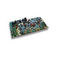
BOARD DEMO FOR ADC1415S125
Manufacturer
NXP Semiconductors
Type
A/Dr
Datasheets
1.ADC1415S125HNC15.pdf
(42 pages)
2.HSDC-ACC01DB.pdf
(32 pages)
3.ADC1415S125DB598.pdf
(2 pages)
Specifications of ADC1415S125/DB,598
Number Of Adc's
1
Number Of Bits
14
Sampling Rate (per Second)
125M
Data Interface
Serial, SPI™
Inputs Per Adc
1 Differential
Input Range
1 ~ 2 Vpp
Power (typ) @ Conditions
840mW @ 125Msps
Voltage Supply Source
Single Supply
Operating Temperature
-40°C ~ 85°C
Utilized Ic / Part
ADC1415S125
Product
Data Conversion Development Tools
Conversion Rate
125 MSPS
Resolution
14 bit
Interface Type
SMA
For Use With/related Products
ADC1415S125
Lead Free Status / RoHS Status
Lead free / RoHS Compliant
Lead Free Status / RoHS Status
Lead free / RoHS Compliant, Lead free / RoHS Compliant
Other names
568-5094


NXP Semiconductors
16. Contents
1
2
3
4
5
6
6.1
6.2
7
8
9
10
10.1
10.2
10.3
10.4
11
11.1
11.1.1
11.1.2
11.1.3
11.1.4
11.2
11.2.1
11.2.2
11.3
11.3.1
11.3.2
11.3.3
11.3.4
11.4
11.4.1
11.4.2
11.4.3
11.4.4
11.5
11.5.1
11.5.2
11.5.3
11.5.4
11.5.5
11.5.6
11.5.7
11.6
11.6.1
11.6.2
General description . . . . . . . . . . . . . . . . . . . . . . 1
Features and benefits . . . . . . . . . . . . . . . . . . . . 1
Applications . . . . . . . . . . . . . . . . . . . . . . . . . . . . 2
Ordering information . . . . . . . . . . . . . . . . . . . . . 2
Block diagram . . . . . . . . . . . . . . . . . . . . . . . . . . 3
Pinning information . . . . . . . . . . . . . . . . . . . . . . 4
Limiting values. . . . . . . . . . . . . . . . . . . . . . . . . . 6
Thermal characteristics . . . . . . . . . . . . . . . . . . 6
Static characteristics. . . . . . . . . . . . . . . . . . . . . 7
Dynamic characteristics . . . . . . . . . . . . . . . . . 10
Application information. . . . . . . . . . . . . . . . . . 17
Clock and digital output timing . . . . . . . . . . . . 12
Device control . . . . . . . . . . . . . . . . . . . . . . . . . 17
Operating mode selection. . . . . . . . . . . . . . . . 18
Selecting the output data format. . . . . . . . . . . 18
Analog inputs . . . . . . . . . . . . . . . . . . . . . . . . . 18
Input stage . . . . . . . . . . . . . . . . . . . . . . . . . . . 18
Transformer . . . . . . . . . . . . . . . . . . . . . . . . . . 20
Programmable full-scale . . . . . . . . . . . . . . . . . 22
Biasing . . . . . . . . . . . . . . . . . . . . . . . . . . . . . . 22
Drive modes . . . . . . . . . . . . . . . . . . . . . . . . . 23
Equivalent input circuit . . . . . . . . . . . . . . . . . . 24
Digital outputs . . . . . . . . . . . . . . . . . . . . . . . . . 25
Digital output buffers: CMOS mode . . . . . . . . 25
Digital output buffers: LVDS DDR mode . . . . . 26
DAta Valid (DAV) output clock . . . . . . . . . . . . 27
Out-of-Range (OTR) . . . . . . . . . . . . . . . . . . . . 27
Digital offset . . . . . . . . . . . . . . . . . . . . . . . . . . 27
Test patterns . . . . . . . . . . . . . . . . . . . . . . . . . . 27
Output codes versus input voltage . . . . . . . . . 28
Register description . . . . . . . . . . . . . . . . . . . . 28
Default modes at start-up . . . . . . . . . . . . . . . . 29
Pinning . . . . . . . . . . . . . . . . . . . . . . . . . . . . . . . 4
Pin description . . . . . . . . . . . . . . . . . . . . . . . . . 4
Dynamic characteristics . . . . . . . . . . . . . . . . . 10
SPI timings . . . . . . . . . . . . . . . . . . . . . . . . . . . 15
Typical characteristics . . . . . . . . . . . . . . . . . . 16
SPI and Pin control modes . . . . . . . . . . . . . . . 17
Selecting the output data standard . . . . . . . . . 18
System reference and power management . . 21
Internal/external references . . . . . . . . . . . . . . 21
Common-mode output voltage (V
Clock input . . . . . . . . . . . . . . . . . . . . . . . . . . . 23
Duty cycle stabilizer . . . . . . . . . . . . . . . . . . . . 24
Clock input divider . . . . . . . . . . . . . . . . . . . . . 24
Serial Peripheral Interface (SPI) . . . . . . . . . . . 28
O(cm)
Single 14-bit ADC; input buffer; CMOS or LVDS DDR digital outputs
) . . . . . 22
11.6.3
12
13
14
14.1
14.2
14.3
14.4
15
16
Please be aware that important notices concerning this document and the product(s)
described herein, have been included in section ‘Legal information’.
© NXP B.V. 2010.
For more information, please visit: http://www.nxp.com
For sales office addresses, please send an email to: salesaddresses@nxp.com
Package outline. . . . . . . . . . . . . . . . . . . . . . . . 38
Revision history . . . . . . . . . . . . . . . . . . . . . . . 39
Legal information . . . . . . . . . . . . . . . . . . . . . . 40
Contact information . . . . . . . . . . . . . . . . . . . . 41
Contents. . . . . . . . . . . . . . . . . . . . . . . . . . . . . . 42
Register allocation map . . . . . . . . . . . . . . . . . 31
Data sheet status . . . . . . . . . . . . . . . . . . . . . . 40
Definitions . . . . . . . . . . . . . . . . . . . . . . . . . . . 40
Disclaimers . . . . . . . . . . . . . . . . . . . . . . . . . . 40
Trademarks . . . . . . . . . . . . . . . . . . . . . . . . . . 41
ADC1415S series
Document identifier: ADC1415S_SER
Date of release: 17 December 2010
All rights reserved.
Related parts for ADC1415S125/DB,598
Image
Part Number
Description
Manufacturer
Datasheet
Request
R

Part Number:
Description:
Single 14-bit ADC
Manufacturer:
NXP Semiconductors
Datasheet:
Part Number:
Description:
NXP Semiconductors designed the LPC2420/2460 microcontroller around a 16-bit/32-bitARM7TDMI-S CPU core with real-time debug interfaces that include both JTAG andembedded trace
Manufacturer:
NXP Semiconductors
Datasheet:

Part Number:
Description:
NXP Semiconductors designed the LPC2458 microcontroller around a 16-bit/32-bitARM7TDMI-S CPU core with real-time debug interfaces that include both JTAG andembedded trace
Manufacturer:
NXP Semiconductors
Datasheet:
Part Number:
Description:
NXP Semiconductors designed the LPC2468 microcontroller around a 16-bit/32-bitARM7TDMI-S CPU core with real-time debug interfaces that include both JTAG andembedded trace
Manufacturer:
NXP Semiconductors
Datasheet:
Part Number:
Description:
NXP Semiconductors designed the LPC2470 microcontroller, powered by theARM7TDMI-S core, to be a highly integrated microcontroller for a wide range ofapplications that require advanced communications and high quality graphic displays
Manufacturer:
NXP Semiconductors
Datasheet:
Part Number:
Description:
NXP Semiconductors designed the LPC2478 microcontroller, powered by theARM7TDMI-S core, to be a highly integrated microcontroller for a wide range ofapplications that require advanced communications and high quality graphic displays
Manufacturer:
NXP Semiconductors
Datasheet:
Part Number:
Description:
The Philips Semiconductors XA (eXtended Architecture) family of 16-bit single-chip microcontrollers is powerful enough to easily handle the requirements of high performance embedded applications, yet inexpensive enough to compete in the market for hi
Manufacturer:
NXP Semiconductors
Datasheet:
Part Number:
Description:
The XA-S3 device is a member of Philips Semiconductors? XA(eXtended Architecture) family of high performance 16-bitsingle-chip microcontrollers
Manufacturer:
NXP Semiconductors
Datasheet:

Part Number:
Description:
The NXP BlueStreak LH75401/LH75411 family consists of two low-cost 16/32-bit System-on-Chip (SoC) devices
Manufacturer:
NXP Semiconductors
Datasheet:
Part Number:
Description:
The NXP LPC3130/3131 combine an 180 MHz ARM926EJ-S CPU core, high-speed USB2
Manufacturer:
NXP Semiconductors
Datasheet:
Part Number:
Description:
The NXP LPC3141 combine a 270 MHz ARM926EJ-S CPU core, High-speed USB 2
Manufacturer:
NXP Semiconductors
Part Number:
Description:
The NXP LPC3143 combine a 270 MHz ARM926EJ-S CPU core, High-speed USB 2
Manufacturer:
NXP Semiconductors

Part Number:
Description:
The NXP LPC3152 combines an 180 MHz ARM926EJ-S CPU core, High-speed USB 2
Manufacturer:
NXP Semiconductors
Part Number:
Description:
The NXP LPC3154 combines an 180 MHz ARM926EJ-S CPU core, High-speed USB 2
Manufacturer:
NXP Semiconductors