CDB5345 Cirrus Logic Inc, CDB5345 Datasheet - Page 2
CDB5345
Manufacturer Part Number
CDB5345
Description
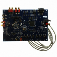
EVALUATION BOARD FOR CS5345
Manufacturer
Cirrus Logic Inc
Specifications of CDB5345
Number Of Adc's
2
Number Of Bits
24
Sampling Rate (per Second)
192k
Data Interface
Serial
Inputs Per Adc
6 Single Ended
Power (typ) @ Conditions
400mW @ 5 V
Voltage Supply Source
Analog and Digital
Operating Temperature
-10°C ~ 70°C
Utilized Ic / Part
CS5345
Description/function
Audio A/D
Operating Supply Voltage
5 V
Product
Audio Modules
For Use With/related Products
CS5345
Lead Free Status / RoHS Status
Contains lead / RoHS non-compliant
Lead Free Status / RoHS Status
Lead free / RoHS Compliant, Contains lead / RoHS non-compliant
Other names
598-1780


2
TABLE OF CONTENTS
1. PIN DESCRIPTIONS
2. CHARACTERISTICS AND SPECIFICATIONS ...................................................................................... 7
3. TYPICAL CONNECTION DIAGRAM ................................................................................................... 22
4. APPLICATIONS ................................................................................................................................... 23
5. REGISTER QUICK REFERENCE ........................................................................................................ 30
6. REGISTER DESCRIPTION .................................................................................................................. 31
4.1 Recommended Power-Up Sequence ............................................................................................. 23
4.2 System Clocking ............................................................................................................................. 23
4.3 High-Pass Filter and DC Offset Calibration .................................................................................... 24
4.4 Analog Input Multiplexer, PGA, and Mic Gain ................................................................................ 25
4.5 Input Connections ........................................................................................................................... 25
4.6 PGA Auxiliary Analog Output ......................................................................................................... 25
4.7 Control Port Description and Timing ............................................................................................... 26
4.8 Interrupts and Overflow .................................................................................................................. 28
4.9 Reset .............................................................................................................................................. 28
4.10 Synchronization of Multiple Devices ............................................................................................. 28
4.11 Grounding and Power Supply Decoupling .................................................................................... 28
6.1 Chip ID - Register 01h .................................................................................................................... 31
6.2 Power Control - Address 02h ......................................................................................................... 31
6.3 ADC Control - Address 04h ............................................................................................................ 32
6.4 MCLK Frequency - Address 05h .................................................................................................... 33
6.5 PGAOut Control - Address 06h ...................................................................................................... 33
6.6 Channel B PGA Control - Address 07h .......................................................................................... 33
SPECIFIED OPERATING CONDITIONS ............................................................................................. 7
ABSOLUTE MAXIMUM RATINGS ....................................................................................................... 7
ADC ANALOG CHARACTERISTICS ................................................................................................... 8
ADC ANALOG CHARACTERISTICS ................................................................................................. 10
ADC DIGITAL FILTER CHARACTERISTICS ..................................................................................... 11
PGAOUT ANALOG CHARACTERISTICS .......................................................................................... 12
PGAOUT ANALOG CHARACTERISTICS .......................................................................................... 13
PGAOUT ANALOG CHARACTERISTICS .......................................................................................... 14
DC ELECTRICAL CHARACTERISTICS ............................................................................................. 15
DIGITAL INTERFACE CHARACTERISTICS ...................................................................................... 16
SWITCHING CHARACTERISTICS - SERIAL AUDIO PORT ............................................................. 17
SWITCHING CHARACTERISTICS - CONTROL PORT - I²C FORMAT ............................................ 20
SWITCHING CHARACTERISTICS - CONTROL PORT - SPI FORMAT ........................................... 21
4.2.1 Master Clock ......................................................................................................................... 23
4.2.2 Master Mode ......................................................................................................................... 24
4.2.3 Slave Mode ........................................................................................................................... 24
4.7.1 SPI Mode ............................................................................................................................... 26
4.7.2 I²C Mode ................................................................................................................................ 26
6.2.1 Freeze (Bit 7) ......................................................................................................................... 31
6.2.2 Power-Down MIC (Bit 3) ........................................................................................................ 31
6.2.3 Power-Down ADC (Bit 2) ....................................................................................................... 31
6.2.4 Power-Down Device (Bit 0) ................................................................................................... 31
6.3.1 Functional Mode (Bits 7:6) .................................................................................................... 32
6.3.2 Digital Interface Format (Bit 4) .............................................................................................. 32
6.3.3 Mute (Bit 2) ............................................................................................................................ 32
6.3.4 High-Pass Filter Freeze (Bit 1) .............................................................................................. 32
6.3.5 Master / Slave Mode (Bit 0) ................................................................................................... 32
6.4.1 Master Clock Dividers (Bits 6:4) ............................................................................................ 33
6.5.1 PGAOut Source Select (Bit 6) ............................................................................................... 33
......................................................................................................................... 5
CS5345
DS658F2
Related parts for CDB5345
Image
Part Number
Description
Manufacturer
Datasheet
Request
R

Part Number:
Description:
Development Kit
Manufacturer:
Cirrus Logic Inc
Datasheet:
Part Number:
Description:
Development Kit
Manufacturer:
Cirrus Logic Inc
Datasheet:


Part Number:
Description:
High-efficiency PFC + Fluorescent Lamp Driver Reference Design
Manufacturer:
Cirrus Logic Inc
Datasheet:
Part Number:
Description:
Development Kit
Manufacturer:
Cirrus Logic Inc
Datasheet:
Part Number:
Description:
Development Kit
Manufacturer:
Cirrus Logic Inc
Datasheet:

Part Number:
Description:
Development Kit
Manufacturer:
Cirrus Logic Inc
Datasheet:
Part Number:
Description:
Development Kit
Manufacturer:
Cirrus Logic Inc
Datasheet:
Part Number:
Description:
Development Kit
Manufacturer:
Cirrus Logic Inc
Datasheet:
Part Number:
Description:
Development Kit
Manufacturer:
Cirrus Logic Inc
Datasheet:

Part Number:
Description:
EVALUATION BOARD FOR CS8427
Manufacturer:
Cirrus Logic Inc
Datasheet:

Part Number:
Description:
BOARD EVAL FOR CS8416 RCVR
Manufacturer:
Cirrus Logic Inc
Datasheet:

Part Number:
Description:
EVALUATION BOARD FOR CS8420
Manufacturer:
Cirrus Logic Inc
Datasheet:

Part Number:
Description:
KIT DEVELOPMENT EP9315 ARM9
Manufacturer:
Cirrus Logic Inc
Datasheet:

Part Number:
Description:
KIT DEVELOPMENT EP9302 ARM9
Manufacturer:
Cirrus Logic Inc
Datasheet: