CDB5345 Cirrus Logic Inc, CDB5345 Datasheet - Page 24
CDB5345
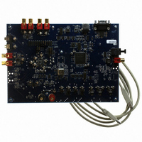
Manufacturer Part Number
CDB5345
Description
EVALUATION BOARD FOR CS5345
Manufacturer
Cirrus Logic Inc
Specifications of CDB5345
Number Of Adc's
2
Number Of Bits
24
Sampling Rate (per Second)
192k
Data Interface
Serial
Inputs Per Adc
6 Single Ended
Power (typ) @ Conditions
400mW @ 5 V
Voltage Supply Source
Analog and Digital
Operating Temperature
-10°C ~ 70°C
Utilized Ic / Part
CS5345
Description/function
Audio A/D
Operating Supply Voltage
5 V
Product
Audio Modules
For Use With/related Products
CS5345
Lead Free Status / RoHS Status
Contains lead / RoHS non-compliant
Lead Free Status / RoHS Status
Lead free / RoHS Compliant, Contains lead / RoHS non-compliant
Other names
598-1780


24
4.2.2
4.2.3
4.3
High-Pass Filter and DC Offset Calibration
When using operational amplifiers in the input circuitry driving the CS5345, a small DC offset may be driven
into the A/D converter. The CS5345 includes a high-pass filter after the decimator to remove any DC offset
which could result in recording a DC level, possibly yielding clicks when switching between devices in a mul-
tichannel system.
The high-pass filter continuously subtracts a measure of the DC offset from the output of the decimation
filter. If the HPFFreeze bit (See
the current value of the DC offset for the each channel is frozen and this DC offset will continue to be sub-
tracted from the conversion result. This feature makes it possible to perform a system DC offset calibration
by:
1. Running the CS5345 with the high-pass filter enabled until the filter settles. See the Digital Filter Char-
2. Disabling the high-pass filter and freezing the stored DC offset.
A system calibration performed in this way will eliminate offsets anywhere in the signal path between the
calibration point and the CS5345.
Master Mode
As a clock master, LRCK and SCLK will operate as outputs. LRCK and SCLK are internally derived from
MCLK with LRCK equal to Fs and SCLK equal to 64 x Fs as shown in
Slave Mode
In Slave Mode, SCLK and LRCK operate as inputs. The Left/Right clock signal must be equal to the sam-
ple rate, Fs, and must be synchronously derived from the supplied master clock, MCLK.
The serial bit clock, SCLK, must be synchronously derived from the master clock, MCLK, and be equal to
128x, 64x, 48x or 32x Fs, depending on the desired speed mode. Refer to
tios.
SCLK/LRCK Ratio
acteristics section for filter settling time.
MCLK
MCLK Freq Bits
“High-Pass Filter Freeze (Bit 1)” on page
Table 3. Slave Mode Serial Bit Clock Ratios
Figure 8. Master Mode Clocking
÷1.5
÷1
÷2
÷3
÷4
32x, 48x, 64x, 128x
Single-Speed
000
001
010
011
100
÷256
÷128
÷64
÷4
÷2
÷1
FM Bits
00
01
10
00
01
10
Double-Speed
32x, 48x, 64x
LRCK
SCLK
32.) is set during normal operation,
Figure
Table 3
8.
for required clock ra-
Quad-Speed
32x, 48x, 64x
CS5345
DS658F2
Related parts for CDB5345
Image
Part Number
Description
Manufacturer
Datasheet
Request
R

Part Number:
Description:
Development Kit
Manufacturer:
Cirrus Logic Inc
Datasheet:
Part Number:
Description:
Development Kit
Manufacturer:
Cirrus Logic Inc
Datasheet:


Part Number:
Description:
High-efficiency PFC + Fluorescent Lamp Driver Reference Design
Manufacturer:
Cirrus Logic Inc
Datasheet:
Part Number:
Description:
Development Kit
Manufacturer:
Cirrus Logic Inc
Datasheet:
Part Number:
Description:
Development Kit
Manufacturer:
Cirrus Logic Inc
Datasheet:

Part Number:
Description:
Development Kit
Manufacturer:
Cirrus Logic Inc
Datasheet:
Part Number:
Description:
Development Kit
Manufacturer:
Cirrus Logic Inc
Datasheet:
Part Number:
Description:
Development Kit
Manufacturer:
Cirrus Logic Inc
Datasheet:
Part Number:
Description:
Development Kit
Manufacturer:
Cirrus Logic Inc
Datasheet:

Part Number:
Description:
EVALUATION BOARD FOR CS8427
Manufacturer:
Cirrus Logic Inc
Datasheet:

Part Number:
Description:
BOARD EVAL FOR CS8416 RCVR
Manufacturer:
Cirrus Logic Inc
Datasheet:

Part Number:
Description:
EVALUATION BOARD FOR CS8420
Manufacturer:
Cirrus Logic Inc
Datasheet:

Part Number:
Description:
KIT DEVELOPMENT EP9315 ARM9
Manufacturer:
Cirrus Logic Inc
Datasheet:

Part Number:
Description:
KIT DEVELOPMENT EP9302 ARM9
Manufacturer:
Cirrus Logic Inc
Datasheet: