CDB5345 Cirrus Logic Inc, CDB5345 Datasheet - Page 26
CDB5345
Manufacturer Part Number
CDB5345
Description
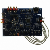
EVALUATION BOARD FOR CS5345
Manufacturer
Cirrus Logic Inc
Specifications of CDB5345
Number Of Adc's
2
Number Of Bits
24
Sampling Rate (per Second)
192k
Data Interface
Serial
Inputs Per Adc
6 Single Ended
Power (typ) @ Conditions
400mW @ 5 V
Voltage Supply Source
Analog and Digital
Operating Temperature
-10°C ~ 70°C
Utilized Ic / Part
CS5345
Description/function
Audio A/D
Operating Supply Voltage
5 V
Product
Audio Modules
For Use With/related Products
CS5345
Lead Free Status / RoHS Status
Contains lead / RoHS non-compliant
Lead Free Status / RoHS Status
Lead free / RoHS Compliant, Contains lead / RoHS non-compliant
Other names
598-1780


26
4.7
4.7.1
4.7.2
CS
C C L K
C D IN
C D O U T
Control Port Description and Timing
The control port is used to access the registers, allowing the CS5345 to be configured for the desired oper-
ational modes and formats. The operation of the control port may be completely asynchronous with respect
to the audio sample rates. However, to avoid potential interference problems, the control port pins should
remain static if no operation is required.
The control port has two modes: SPI and I²C, with the CS5345 acting as a slave device. SPI Mode is se-
lected if there is a high-to-low transition on the AD0/CS pin, after the RESET pin has been brought high. I²C
Mode is selected by connecting the AD0/CS pin through a resistor to VLC or DGND, thereby permanently
selecting the desired AD0 bit address state.
SPI Mode
In SPI Mode, CS is the CS5345 chip-select signal; CCLK is the control port bit clock (input into the CS5345
from the microcontroller); CDIN is the input data line from the microcontroller; CDOUT is the output data
line to the microcontroller. Data is clocked in on the rising edge of CCLK and out on the falling edge.
Figure 10
first seven bits on CDIN form the chip address and must be 1001111. The eighth bit is a read/write indi-
cator (R/W), which should be low to write. The next eight bits form the Memory Address Pointer (MAP),
which is set to the address of the register that is to be updated. The next eight bits are the data that will
be placed into the register designated by the MAP. During writes, the CDOUT output stays in the Hi-Z
state. It may be externally pulled high or low with a 47 kΩ resistor, if desired.
To read a register, the MAP has to be set to the correct address by executing a partial write cycle which
finishes (CS high) immediately after the MAP byte. To begin a read, bring CS low, send out the chip ad-
dress and set the read/write bit (R/W) high. The next falling edge of CCLK will clock out the MSB of the
addressed register (CDOUT will leave the high-impedance state).
For both read and write cycles, the memory address pointer will automatically increment following each
data byte in order to facilitate block reads and writes of successive registers.
I²C Mode
In I²C Mode, SDA is a bidirectional data line. Data is clocked into and out of the part by the clock, SCL.
There is no CS pin. Pins AD0 and AD1 form the two least-significant bits of the chip address and should
ADDRESS
MAP = Memory Address Pointer, 8 bits, MSB first
1001111
C H IP
shows the operation of the control port in SPI Mode. To write to a register, bring CS low. The
High Impedance
R/W
M A P
Figure 10. Control Port Timing in SPI Mode
MSB
b y te 1
DATA
b y te n
LSB
A D D R E S S
C H IP
1001111
R/W
MSB
LSB MSB
CS5345
LSB
DS658F2
Related parts for CDB5345
Image
Part Number
Description
Manufacturer
Datasheet
Request
R

Part Number:
Description:
Development Kit
Manufacturer:
Cirrus Logic Inc
Datasheet:
Part Number:
Description:
Development Kit
Manufacturer:
Cirrus Logic Inc
Datasheet:


Part Number:
Description:
High-efficiency PFC + Fluorescent Lamp Driver Reference Design
Manufacturer:
Cirrus Logic Inc
Datasheet:
Part Number:
Description:
Development Kit
Manufacturer:
Cirrus Logic Inc
Datasheet:
Part Number:
Description:
Development Kit
Manufacturer:
Cirrus Logic Inc
Datasheet:

Part Number:
Description:
Development Kit
Manufacturer:
Cirrus Logic Inc
Datasheet:
Part Number:
Description:
Development Kit
Manufacturer:
Cirrus Logic Inc
Datasheet:
Part Number:
Description:
Development Kit
Manufacturer:
Cirrus Logic Inc
Datasheet:
Part Number:
Description:
Development Kit
Manufacturer:
Cirrus Logic Inc
Datasheet:

Part Number:
Description:
EVALUATION BOARD FOR CS8427
Manufacturer:
Cirrus Logic Inc
Datasheet:

Part Number:
Description:
BOARD EVAL FOR CS8416 RCVR
Manufacturer:
Cirrus Logic Inc
Datasheet:

Part Number:
Description:
EVALUATION BOARD FOR CS8420
Manufacturer:
Cirrus Logic Inc
Datasheet:

Part Number:
Description:
KIT DEVELOPMENT EP9315 ARM9
Manufacturer:
Cirrus Logic Inc
Datasheet:

Part Number:
Description:
KIT DEVELOPMENT EP9302 ARM9
Manufacturer:
Cirrus Logic Inc
Datasheet: