CDB5345 Cirrus Logic Inc, CDB5345 Datasheet - Page 3
CDB5345
Manufacturer Part Number
CDB5345
Description
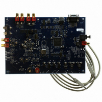
EVALUATION BOARD FOR CS5345
Manufacturer
Cirrus Logic Inc
Specifications of CDB5345
Number Of Adc's
2
Number Of Bits
24
Sampling Rate (per Second)
192k
Data Interface
Serial
Inputs Per Adc
6 Single Ended
Power (typ) @ Conditions
400mW @ 5 V
Voltage Supply Source
Analog and Digital
Operating Temperature
-10°C ~ 70°C
Utilized Ic / Part
CS5345
Description/function
Audio A/D
Operating Supply Voltage
5 V
Product
Audio Modules
For Use With/related Products
CS5345
Lead Free Status / RoHS Status
Contains lead / RoHS non-compliant
Lead Free Status / RoHS Status
Lead free / RoHS Compliant, Contains lead / RoHS non-compliant
Other names
598-1780


DS658F2
LIST OF FIGURES
LIST OF TABLES
7. PARAMETER DEFINITIONS ................................................................................................................ 37
8. FILTER PLOTS
9. PACKAGE DIMENSIONS .................................................................................................................... 40
10. THERMAL CHARACTERISTICS AND SPECIFICATIONS ............................................................. 40
11. ORDERING INFORMATION
12. REVISION HISTORY .......................................................................................................................... 41
Figure 1.Master Mode Serial Audio Port Timing ....................................................................................... 18
Figure 2.Slave Mode Serial Audio Port Timing ......................................................................................... 18
Figure 3.Format 0, Left-Justified up to 24-Bit Data ................................................................................... 19
Figure 4.Format 1, I²S up to 24-Bit Data ................................................................................................... 19
Figure 5.Control Port Timing - I²C Format ................................................................................................. 20
Figure 6.Control Port Timing - SPI Format ................................................................................................ 21
Figure 7.Typical Connection Diagram ....................................................................................................... 22
Figure 8.Master Mode Clocking ................................................................................................................ 24
Figure 9.Analog Input Architecture ............................................................................................................ 25
Figure 10.Control Port Timing in SPI Mode .............................................................................................. 26
Figure 11.Control Port Timing, I²C Write ................................................................................................... 27
Figure 12.Control Port Timing, I²C Read ................................................................................................... 27
Figure 13.Single-Speed Stopband Rejection ............................................................................................ 38
Figure 14.Single-Speed Stopband Rejection ............................................................................................ 38
Figure 15.Single-Speed Transition Band (Detail) ...................................................................................... 38
Figure 16.Single-Speed Passband Ripple ................................................................................................ 38
Figure 17.Double-Speed Stopband Rejection ........................................................................................... 38
Figure 18.Double-Speed Stopband Rejection ........................................................................................... 38
Figure 19.Double-Speed Transition Band (Detail) .................................................................................... 39
Figure 20.Double-Speed Passband Ripple ............................................................................................... 39
Figure 21.Quad-Speed Stopband Rejection ............................................................................................. 39
Figure 22.Quad-Speed Stopband Rejection ............................................................................................. 39
Figure 23.Quad-Speed Transition Band (Detail) ....................................................................................... 39
Figure 24.Quad-Speed Passband Ripple ................................................................................................. 39
Table 1. Speed Modes .............................................................................................................................. 23
Table 2. Common Clock Frequencies ....................................................................................................... 23
Table 3. Slave Mode Serial Bit Clock Ratios ............................................................................................. 24
Table 4. Device Revision .......................................................................................................................... 31
6.7 Channel A PGA Control - Address 08h .......................................................................................... 34
6.8 ADC Input Control - Address 09h ................................................................................................... 34
6.9 Active Level Control - Address 0Ch ................................................................................................ 35
6.10 Interrupt Status - Address 0Dh ..................................................................................................... 35
6.11 Interrupt Mask - Address 0Eh ....................................................................................................... 36
6.12 Interrupt Mode MSB - Address 0Fh .............................................................................................. 36
6.13 Interrupt Mode LSB - Address 10h ............................................................................................... 36
6.6.1 Channel B PGA Gain (Bits 5:0) ............................................................................................. 33
6.7.1 Channel A PGA Gain (Bits 5:0) ............................................................................................. 34
6.8.1 PGA Soft Ramp or Zero Cross Enable (Bits 4:3) .................................................................. 34
6.8.2 Analog Input Selection (Bits 2:0) ........................................................................................... 35
6.9.1 Active High/Low (Bit 0) .......................................................................................................... 35
6.10.1 Clock Error (Bit 3) ................................................................................................................ 36
6.10.2 Overflow (Bit 1) .................................................................................................................... 36
6.10.3 Underflow (Bit 0) .................................................................................................................. 36
.................................................................................................................................. 38
........................................................................................................ 41
CS5345
3
Related parts for CDB5345
Image
Part Number
Description
Manufacturer
Datasheet
Request
R

Part Number:
Description:
Development Kit
Manufacturer:
Cirrus Logic Inc
Datasheet:
Part Number:
Description:
Development Kit
Manufacturer:
Cirrus Logic Inc
Datasheet:


Part Number:
Description:
High-efficiency PFC + Fluorescent Lamp Driver Reference Design
Manufacturer:
Cirrus Logic Inc
Datasheet:
Part Number:
Description:
Development Kit
Manufacturer:
Cirrus Logic Inc
Datasheet:
Part Number:
Description:
Development Kit
Manufacturer:
Cirrus Logic Inc
Datasheet:

Part Number:
Description:
Development Kit
Manufacturer:
Cirrus Logic Inc
Datasheet:
Part Number:
Description:
Development Kit
Manufacturer:
Cirrus Logic Inc
Datasheet:
Part Number:
Description:
Development Kit
Manufacturer:
Cirrus Logic Inc
Datasheet:
Part Number:
Description:
Development Kit
Manufacturer:
Cirrus Logic Inc
Datasheet:

Part Number:
Description:
EVALUATION BOARD FOR CS8427
Manufacturer:
Cirrus Logic Inc
Datasheet:

Part Number:
Description:
BOARD EVAL FOR CS8416 RCVR
Manufacturer:
Cirrus Logic Inc
Datasheet:

Part Number:
Description:
EVALUATION BOARD FOR CS8420
Manufacturer:
Cirrus Logic Inc
Datasheet:

Part Number:
Description:
KIT DEVELOPMENT EP9315 ARM9
Manufacturer:
Cirrus Logic Inc
Datasheet:

Part Number:
Description:
KIT DEVELOPMENT EP9302 ARM9
Manufacturer:
Cirrus Logic Inc
Datasheet: