RDK-115 Power Integrations, RDK-115 Datasheet - Page 8
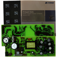
RDK-115
Manufacturer Part Number
RDK-115
Description
KIT REFERENCE DESIGN W/TN376PN
Manufacturer
Power Integrations
Series
TinySwitch®-PKr
Specifications of RDK-115
Main Purpose
AC/DC, Primary Side
Outputs And Type
4, Isolated
Power - Output
7.5W
Voltage - Output
3.3V, 5V, 12V, -12V
Current - Output
500mA, 500mA, 250mA, 30mA
Voltage - Input
85 ~ 265VAC
Regulator Topology
Flyback
Frequency - Switching
132kHz
Board Type
Fully Populated
Utilized Ic / Part
TNY376
Product
Accessories & Kits
Lead Free Status / RoHS Status
Not applicable / Not applicable
Other names
596-1145


4 Circuit Description
4.1 Input EMI Filtering
One requirement of this design was to meet conducted EMI with the output return
connected to safety earth ground. This simulates the condition where the DVD player or
set-top box is earth grounded either by an antenna or cable TV input cable.
The EMI filtering consists of a π filter formed by C1, L1 and C4 together with capacitor
C8. A common mode choke was selected over discrete inductors for L1 to meet the earth
grounded requirement. Such a simple arrangement was possible due to the switching
frequency jitter feature of U4 and the E-Shield™ techniques used in the transformer.
Provision for an additional X class capacitor (C3) is made on the board but is not
required.
4.2 TinySwitch-PK Primary
The TNY376 (U4) has the following functions integrated onto a monolithic IC: a 700 V
power MOSFET, a low-voltage CMOS controller, a high-voltage current source (provides
startup and steady-state operational current to the IC), hysteretic thermal shutdown, and
auto-restart. The excellent switching characteristics of the integrated power MOSFET
allow efficient operation up to 132 kHz (264 kHz in Peak Power Mode).
Under normal operation, the rectified and filtered input voltage is applied to one side of
the primary winding of T1. The other side of the T1 primary winding is connected to the
DRAIN pin of U4. As soon as the voltage is applied across the DRAIN and SOURCE
pins of U4, the internal high voltage current source (connected to the DRAIN pin of the
IC) begins charging the capacitor (C19) connected to the BYPASS/MULTIFUNCTION
(BP/M) pin. Once the voltage across C19 reaches 5.8 V, the controller enables MOSFET
switching. MOSFET current is sensed (internally) by the voltage developed across the
Drain to Source resistance (R
preset (internal) current-limit trip point (I
The controller regulates the output voltage by skipping switching cycles (ON/OFF control)
whenever the output voltage is above the reference level. During normal operation,
MOSFET switching is disabled whenever the current flowing out of the EN/UV pin is
greater than 90 µA. If less than 90 µA is flowing out of the EN/UV pin when the
oscillator’s (internal) clock signal occurs, MOSFET switching is enabled for that switching
cycle, and the MOSFET turns on. That switching cycle terminates when the current
through the MOSFET reaches I
switching cycles will be skipped (disabled) resulting in a high effective switching
frequency. As the load reduces, more switching cycles are skipped, which reduces the
effective switching frequency. At no-load, most switching cycles are skipped, which is
what makes the no-load power consumption of supplies designed around the
TinySwitch-PK family so low, since switching losses are the dominant loss mechanism at
light loading. Additionally, since the amount of energy per switching cycle is fixed by
Power Integrations
Tel: +1 408 414 9200 Fax: +1 408 414 9201
www.powerint.com
DS(ON)
LIMIT
) while it is turned on. When the current reaches the
, or the DC
LIMIT
), the controller turns the MOSFET off.
MAX
signal is encountered. At full load, few
Page 8 of 36
Related parts for RDK-115
Image
Part Number
Description
Manufacturer
Datasheet
Request
R

Part Number:
Description:
KIT REF DESIGN FOR LNK457D
Manufacturer:
Power Integrations
Datasheet:

Part Number:
Description:
REFERENCE DESIGN LINKSWITCH-PH
Manufacturer:
Power Integrations
Datasheet:

Part Number:
Description:
KIT REF DESIGN FOR LNK403EG
Manufacturer:
Power Integrations
Datasheet:

Part Number:
Description:
KIT REF DESIGN FOR LNK406EG
Manufacturer:
Power Integrations
Datasheet:

Part Number:
Description:
KIT REF DESIGN LINKSWITCH-CV
Manufacturer:
Power Integrations
Datasheet:

Part Number:
Description:
KIT REF DESIGN LINKSWITCH 2
Manufacturer:
Power Integrations
Datasheet:

Part Number:
Description:
Specifications: Family: Eval Boards - DC/DC & AC/DC (Off-Line) SMPS ; Series: HiperLCS™ ; Main Purpose: DC/DC, Step Down ; Outputs and Type: 1, Isolated ; Power - Output: 150W ; Voltage - Output: 24V ; Current - Output: 6.25A ; Voltage - Input:
Manufacturer:
Power Integrations, Inc.
Datasheet:

Part Number:
Description:
KIT DESIGN REF TINYSWITCH-III
Manufacturer:
Power Integrations
Datasheet:

Part Number:
Description:
KIT DESIGN REF LINKSWITCH LP
Manufacturer:
Power Integrations
Datasheet:

Part Number:
Description:
KIT REF DESIGN LED LINKSWITCH TN
Manufacturer:
Power Integrations
Datasheet:
Part Number:
Description:
KIT REF DESIGN PG LINKSWITCH-II
Manufacturer:
Power Integrations
Datasheet:
Part Number:
Description:
REFERENCE DESIGN LINKSWITCH-PL
Manufacturer:
Power Integrations
Datasheet:
Part Number:
Description:
REFERENCE DESIGN LINKSWITCH-PH
Manufacturer:
Power Integrations
Datasheet:

Part Number:
Description:
KIT REF DESIGN 36-72W MOTOR DRVR
Manufacturer:
Power Integrations
Datasheet:
Part Number:
Description:
Specifications: Manufacturer: Power Integrations ; Output Voltage: 380 VDC ; Input / Supply Voltage (Max): 264 VAC ; Input / Supply Voltage (Min): 90 VAC ; Mounting Style: Through Hole ; Output Current: 0.913 A ; Output Power: 347 W
Manufacturer:
Power Integrations, Inc.