STEVAL-ISA050V1 STMicroelectronics, STEVAL-ISA050V1 Datasheet - Page 21
STEVAL-ISA050V1
Manufacturer Part Number
STEVAL-ISA050V1
Description
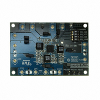
KIT EVAL PM6641 CHIPSET/DDR2/3
Manufacturer
STMicroelectronics
Type
DC/DC Switching Converters, Regulators & Controllersr
Specifications of STEVAL-ISA050V1
Main Purpose
Special Purpose DC/DC, DDR Memory Supply
Outputs And Type
4, Non-Isolated
Power - Output
14.7W
Voltage - Output
1.05V, 1.5V, 1.8V, 0.9V
Current - Output
4A, 2.8A, 2.5A, 2A
Voltage - Input
2.7 ~ 5.5V
Regulator Topology
Buck
Frequency - Switching
750kHz
Board Type
Fully Populated
Utilized Ic / Part
PM6641
Input Voltage
2.7 V to 5.5 V
Product
Power Management Modules
Silicon Manufacturer
ST Micro
Silicon Core Number
PM6641
Kit Application Type
Power Management - Voltage Regulator
Application Sub Type
Monolithic Voltage Regulator
Kit Contents
Board
Lead Free Status / RoHS Status
Lead free / RoHS Compliant
For Use With/related Products
PM6641
Other names
497-8425
Available stocks
Company
Part Number
Manufacturer
Quantity
Price
Company:

Part Number:
STEVAL-ISA050V1
Manufacturer:
STMicroelectronics
Quantity:
1


PM6641
7.1.2
7.1.3
the loop voltage reference is increased linearly from zero up to 0.8V in a long time (up to a
couple of milliseconds) (see
When the EN_1S8 pin goes low, the VDDQ rail output capacitor is discharged through
internal discharge MOSFET and, at the end of the capacitor discharge, the low side power
MOSFET is eventually closed (see
The Power Good signal (PG_1S8 pin) is an open drain output, shorting the output to GND in
the following conditions:
●
●
●
When VDDQ and VTT rails are enabled, PG_1S8 is left floating and, as a consequence,
pulled-up by the external pull-up resistor, if both the rails are inside +/- 10% range of nominal
value. The PG_1S8 pin can sink current up to 4 mA when it’s asserted low.
VTT LDO and VTTREF buffered reference
The PM6641 provides the required DDR2/3 reference voltage on VTTREF pin. The internal
buffer tracks half the voltage on VOUT_1S8 pin and has a sink and source capability up to
15 mA with an accuracy of ±2% referred to the VDDQ half.
Higher currents rapidly deteriorate the output accuracy. A 10 nF to 100 nF (33 nF typical)
bypass capacitor to SGND is required for stability.
The VTT low-drop-out linear regulator has been designed to sink and source up to 2 A peak
current and 1 A continuously. The VTT voltage tracks VTTREF within ±35 mV. A remote
voltage sensing pin (VTTFB) is provided to recovery voltage drops due to parasitic
resistance. In DDR2/3 applications, the linear regulator input LDOIN is typically connected
to VDDQ output; connecting LDOIN pin to a lower voltage (if available in the system)
reduces the power dissipation of the LDO, but a minimum drop-out voltage must be
guaranteed, depending on the maximum current expected.
A minimum output capacitance of 20 µF (2x10 µF or single 22 µF ceramic capacitors) is
enough to assure stability and fast load transient response.
According to DDR2/3 JEDEC specifications, when the system enters the suspend-to-RAM
state (S5 high and S3 low) the LDO output is left in high-impedance while VTTREF and
VDDQ are still alive. When the suspend-to-disk state (S3 and S5 tied to ground) is entered,
all outputs are actively discharged by a tracking or a non-tracking discharge as selected
through the DSCG pin (see
VTT and VTTREF soft-start
Soft-start on VTT and VTTREF outputs is achieved by current clamping. The LDO linear
regulator is provided of a current fold-back protection: when the output voltage exits the
internal ±10% VTT-Good window, the output current is clamped at ±1 A. Re-entering VTT-
Good window releases the current limit clamping. The fold-back mechanism naturally
implements a two steps soft-start charging the output capacitors with a 1 A constant current.
Something similar occurs at VTTREF pin, where the output capacitor is smoothly charged at
a fixed 40 mA (typ) current limit.
When the 1.8 V rail output voltage is outside +/- 10% range from nominal value
When a protection (UV, OV, thermal) has been triggered
When the regulator is in soft-start.
Chapter 7.7: Outputs soft-end on page 29
Chapter 7.6: Outputs soft-start on page 28
Doc ID 13510 Rev 3
Chapter 7.7: Outputs soft-end on page 29
for details).
Device description
for details).
for details).
21/47
Related parts for STEVAL-ISA050V1
Image
Part Number
Description
Manufacturer
Datasheet
Request
R

Part Number:
Description:
BOARD RGB CTR ST7,STP08C596MTR
Manufacturer:
STMicroelectronics
Datasheet:

Part Number:
Description:
Power Management IC Development Tools Full Speed USB to RS232 Bridge Demo
Manufacturer:
STMicroelectronics
Datasheet:
Part Number:
Description:
Power Management IC Development Tools 2.5W solar eval BRD USB SPV1040 LD39050
Manufacturer:
STMicroelectronics
Datasheet:

Part Number:
Description:
BOARD EVAL FOR MEMS SENSORS
Manufacturer:
STMicroelectronics
Datasheet:

Part Number:
Description:
KIT DEV STARTER ST10F276Z5
Manufacturer:
STMicroelectronics
Datasheet:

Part Number:
Description:
BOARD EVAL HDMI $ VIDEO SWITCH
Manufacturer:
STMicroelectronics
Datasheet:

Part Number:
Description:
BOARD DEMO ACCELEROMETER DIL24
Manufacturer:
STMicroelectronics
Datasheet:

Part Number:
Description:
BOARD STLM75/STDS75/ST72F651
Manufacturer:
STMicroelectronics
Datasheet:

Part Number:
Description:
EVAL BOARD 3AXIS MEMS ACCELLRMTR
Manufacturer:
STMicroelectronics
Datasheet:

Part Number:
Description:
BOARD EVAL 8BIT MICRO + TDE1708
Manufacturer:
STMicroelectronics
Datasheet:
Part Number:
Description:
STMicroelectronics [RIPPLE-CARRY BINARY COUNTER/DIVIDERS]
Manufacturer:
STMicroelectronics
Datasheet:
Part Number:
Description:
STMicroelectronics [LIQUID-CRYSTAL DISPLAY DRIVERS]
Manufacturer:
STMicroelectronics
Datasheet:
Part Number:
Description:
BOARD EVAL FOR MEMS SENSORS
Manufacturer:
STMicroelectronics
Datasheet: