STEVAL-ISA050V1 STMicroelectronics, STEVAL-ISA050V1 Datasheet - Page 31
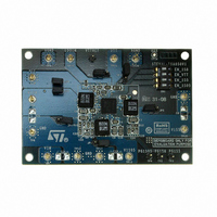
STEVAL-ISA050V1
Manufacturer Part Number
STEVAL-ISA050V1
Description
KIT EVAL PM6641 CHIPSET/DDR2/3
Manufacturer
STMicroelectronics
Type
DC/DC Switching Converters, Regulators & Controllersr
Specifications of STEVAL-ISA050V1
Main Purpose
Special Purpose DC/DC, DDR Memory Supply
Outputs And Type
4, Non-Isolated
Power - Output
14.7W
Voltage - Output
1.05V, 1.5V, 1.8V, 0.9V
Current - Output
4A, 2.8A, 2.5A, 2A
Voltage - Input
2.7 ~ 5.5V
Regulator Topology
Buck
Frequency - Switching
750kHz
Board Type
Fully Populated
Utilized Ic / Part
PM6641
Input Voltage
2.7 V to 5.5 V
Product
Power Management Modules
Silicon Manufacturer
ST Micro
Silicon Core Number
PM6641
Kit Application Type
Power Management - Voltage Regulator
Application Sub Type
Monolithic Voltage Regulator
Kit Contents
Board
Lead Free Status / RoHS Status
Lead free / RoHS Compliant
For Use With/related Products
PM6641
Other names
497-8425
Available stocks
Company
Part Number
Manufacturer
Quantity
Price
Company:

Part Number:
STEVAL-ISA050V1
Manufacturer:
STMicroelectronics
Quantity:
1


PM6641
7.10
The synchronous mode of operation provides the following total input current:
Equation 8
whereas by shifting the three regulator turn on pulses of 120 deg the resulting total input
current is given by
Equation 9
that is
The PM6641 SET_PH1 pin, if tied to AVCC, enables the synchronous switching regulators
high side MOSFET turn on, whereas if tied to ground enables the 120 deg phase shifting.
Peak current limit
The peak current limit performed by the PM6641 switching regulators allows to monitor,
cycle by cycle, the inductor current; this feature prevents IC wire bonding overheating and
failure.
If the current sensed on the monolithic high side MOSFET reaches the programmed current
limit the regulator starts behaving like a current generator, more than a voltage regulator.
Consequently, if the output load still increases the rail output capacitor discharges itself and
the regulator works as current generator until the output under voltage occurs and the
regulator is latched off (see
details).
The pin 4 (CSNS) allows to select the right value for the peak current limit by inserting an
external resistor (R
RCSNS resistor or, when tied to AVCC, enables the internal reference (equal to a 50 kΩ
external resistor). A simple equation shows how to compute the right value for R
order to decrease the peak current limit:
Equation 10
3 ≅
. 1
73
I
CIN
,
times smaller than the one computed before.
I
DELAY
CSNS
CIN
,
SYNC
) between this pin and ground. CSNS forces a constant voltage on
=
=
Chapter 7.11.2: Output under voltage on page 33
T
SW
1
Doc ID 13510 Rev 3
T
SW
1
T
∫
SW
(
T
I
L
SW
∫
R
1
(
CSNS
I
+
L
1
I
L
+
2
I
+
L
=
2
I
L
α
+
3
⋅
I
)
L
2
V
3
I
dt
REF
CL
)
2
=
dt
=
T
SW
1
T
SW
1
(
I
2
+
( )
I 3
I
2
2
+
T
I
ON
2
Device description
)
T
ON
section for
CSNS
in
31/47
Related parts for STEVAL-ISA050V1
Image
Part Number
Description
Manufacturer
Datasheet
Request
R

Part Number:
Description:
BOARD RGB CTR ST7,STP08C596MTR
Manufacturer:
STMicroelectronics
Datasheet:

Part Number:
Description:
Power Management IC Development Tools Full Speed USB to RS232 Bridge Demo
Manufacturer:
STMicroelectronics
Datasheet:
Part Number:
Description:
Power Management IC Development Tools 2.5W solar eval BRD USB SPV1040 LD39050
Manufacturer:
STMicroelectronics
Datasheet:

Part Number:
Description:
BOARD EVAL FOR MEMS SENSORS
Manufacturer:
STMicroelectronics
Datasheet:

Part Number:
Description:
KIT DEV STARTER ST10F276Z5
Manufacturer:
STMicroelectronics
Datasheet:

Part Number:
Description:
BOARD EVAL HDMI $ VIDEO SWITCH
Manufacturer:
STMicroelectronics
Datasheet:

Part Number:
Description:
BOARD DEMO ACCELEROMETER DIL24
Manufacturer:
STMicroelectronics
Datasheet:

Part Number:
Description:
BOARD STLM75/STDS75/ST72F651
Manufacturer:
STMicroelectronics
Datasheet:

Part Number:
Description:
EVAL BOARD 3AXIS MEMS ACCELLRMTR
Manufacturer:
STMicroelectronics
Datasheet:

Part Number:
Description:
BOARD EVAL 8BIT MICRO + TDE1708
Manufacturer:
STMicroelectronics
Datasheet:
Part Number:
Description:
STMicroelectronics [RIPPLE-CARRY BINARY COUNTER/DIVIDERS]
Manufacturer:
STMicroelectronics
Datasheet:
Part Number:
Description:
STMicroelectronics [LIQUID-CRYSTAL DISPLAY DRIVERS]
Manufacturer:
STMicroelectronics
Datasheet:
Part Number:
Description:
BOARD EVAL FOR MEMS SENSORS
Manufacturer:
STMicroelectronics
Datasheet: