STEVAL-ISA019V2 STMicroelectronics, STEVAL-ISA019V2 Datasheet
STEVAL-ISA019V2
Specifications of STEVAL-ISA019V2


Related parts for STEVAL-ISA019V2


STEVAL-ISA019V2 Summary of contents
Page 1
... The input voltage can also be extended up to 1000 VDC as enough margin exists to do so. Finally, the experimental results are analyzed to better understand the benefits offered by the use of ESBT in this application. The document is associated with demonstration boards STEVAL-ISA019V1 and STEVAL- ISA019V2 (Figure Figure 1 ...
Page 2
Contents Contents 1 Design specifications and L6565 brief description . . . . . . . . . . . . . . . . 4 2 Flyback stage design . . . . . . . . . . ...
Page 3
... Figure 18. Proportional base driving circuit relevant waveform . . . . . . . . . . . . . . . . . . . . . . . . . . . . . 24 Figure 19. PCB layout (top view Figure 20. PCB layout (bottom view Figure 21. STEVAL-ISA019V2 Figure 22. STEVAL-ISA019V2 schematic diagram . . . . . . . . . . . . . . . . . . . . . . . . . . . . . . . . . . . . . . . 29 Figure 23. Power transformer Delta 86H-6017 . . . . . . . . . . . . . . . . . . . . . . . . . . . . . . . . . . . . . . . . . . 30 Figure 24. Silk screen (top side Figure 25. Silk screen (bottom side Figure 26. Copper tracks . . . . . . . . . . . . . . . . . . . . . . . . . . . . . . . . . . . . . . . . . . . . . . . . . . . . . . . . . . . 31 ...
Page 4
Design specifications and L6565 brief description 1 Design specifications and L6565 brief description Table 1 lists the converter specification data and the main parameters set for the demonstration board. Table 1. Converter specification data and fixed parameters Symbol V inmin ...
Page 5
AN2495 2 Flyback stage design In Figure 3 the complete schematic of the 80 W SMPS is shown. Figure 3. Demonstration board schematic Doc ID 13127 Rev 4 Flyback stage design 5/34 ...
Page 6
Flyback stage design As commonly known, the voltage stress on the device (power switch) is given by: Equation 1 where V = flyback voltage = (V fl allowed by the clamping network. It has been set at 200 V. N ...
Page 7
AN2495 Hence: Equation 8 Now we can calculate the peak current on primary. Equation 9 2.1 Transformer design 2.1.1 Core size The core size must be chosen according to the power that must be managed, to the primary inductance, and ...
Page 8
Flyback stage design Figure 4. Dynamic magnetization curves Concerning the gap, from the EPCOS datasheet, we can use the following approximate formula: Equation 153 -0.713, while Knowing that L = 1.56mH and ...
Page 9
AN2495 Figure 5. Relative core losses versus frequency From Figure 5, operating at 50 kHz with 220 mT flux excursion, the power dissipation density is about 300 mW/cm ETD 34 is 7.63 cm Equation 14 Assuming a 95% efficiency for ...
Page 10
Flyback stage design Equation 18 A SCU Table 2 provides the skin effect resistance ratios due to eddy currents for different frequencies. Table 2. Skin effect AC-DC resistance ratios for square-wave currents 25 kHz Skin wire Diameter depth S, d/S ...
Page 11
AN2495 Figure 6. Power transformer Tronic 0600387 Doc ID 13127 Rev 4 Flyback stage design Top view 11/34 ...
Page 12
Base driving circuit design 3 Base driving circuit design In practical applications such as SMPS where the load is variable, the collector current is variable as well consequence it is very important to provide a base current to ...
Page 13
AN2495 During the conduction time, the junction base-emitter of the ESBT can be seen as a forward-biased diode. To complete the secondary side load loop, the voltage drop on both diode D and resistor RB must be added in series ...
Page 14
Base driving circuit design I must be limited to avoid extra saturation of the device. The Zener diode D peak and clamps the voltage across the small capacitor C to the following empirical formulas and inside the range of V ...
Page 15
AN2495 Figure 8. Current transformer SL 051 220 21 01 Section Bottom view Doc ID 13127 Rev 4 Base driving circuit design Equivalent schematic 15/34 ...
Page 16
Output circuit design 4 Output circuit design To choose the output capacitor, the series resistance of the electrolytic capacitor must be defined well known that the main cause of the output ripple is the series resistance of the ...
Page 17
AN2495 5 Startup network design To allow the circuit to start as soon as the line voltage is applied necessary to pre- charge both C and resistor connected to the DC bus directly makes the ...
Page 18
Frequency response and loop compensation 6 Frequency response and loop compensation The transfer function in the complex frequency domain of the discontinuous current mode (DCM) flyback converter with L6565 driver is given by: Equation 36 V out ...
Page 19
AN2495 Figure 9. Converter feedback network Its transfer function, which comprises a pole at the origin and a zero-pole pair, is given by: Equation 38 G The task of the control loop design is then to determine the transfer function ...
Page 20
Frequency response and loop compensation The resistive partition must be set with high precision according to the following formula: Equation 40 There is no next close commercial value good idea to put two 47 kΩ resistors ...
Page 21
AN2495 7 Efficiency, waveforms and experimental results Overall efficiency variation versus output power is illustrated in values of input voltage. Figure 11. Overall efficiency versus output power for two different values of input voltage It is worth noting that with ...
Page 22
Efficiency, waveforms and experimental results Figure 12. Minimum input voltage-maximum load (250 V- steady state Figure 13. Medium input voltage-maximum load (500 V- steady state 22/34 Doc ID 13127 Rev 4 AN2495 ...
Page 23
AN2495 Figure 14. Maximum input voltage-maximum load (850 V- steady state Waveforms in Figure both low and high load conditions with the same input rectified voltage. Figure 15. Very low load condition (750 V-5 W) Figure 16. Low ...
Page 24
Efficiency, waveforms and experimental results Figure 17. High load condition (750 V-80 W) The waveform in In this graph, collector current is the violet line, while the base current line is sky blue. Figure 18. Proportional base driving circuit relevant ...
Page 25
AN2495 8 PCB layout and list of material The PCB (printed circuit board) is shown in Figure 19. PCB layout (top view) Figure 20. PCB layout (bottom view) PCB layout and list of material Figure 19 and Figure Doc ID ...
Page 26
Bill of material 9 Bill of material Table 4. Bill of material D1,D2,D3,D4 R1, R2, R3, R4 26/34 Part C1,C2 C3, C10 C11 C12 C13 D5 D6 D7,D8,D10 D9 D11 R5 R6, R7 R8, R9, ...
Page 27
AN2495 Table 4. Bill of material (continued) Part R24 Q1 J1 ISO1 F1 Fuse holder T1 T2 het1, het2 Doc ID 13127 Rev 4 Bill of material Description 1.5 kΩ/0.25 W STC04IE170HV ARK700I/2 ARK500/2 L6565 TL431 ...
Page 28
... Board modifications This paragraph has been added following the release of a more recent version of the board (STEVAL-ISA019V2). For the design procedure and rules, all the preceding paragraphs remain valid. Working conditions have not been changed. The new version was released to take advantage of the size reduction of the SMD components and to insert a new transformer with better coupling between primary inductance and auxiliary winding ...
Page 29
... AN2495 Figure 22. STEVAL-ISA019V2 schematic diagram 450V The specifications of the transformer provided by Delta Electronics Inc. are shown in Figure 23. 1 220u 450V 220u Doc ID 13127 Rev 4 Board modifications ZCD GND 5 6 VCC INV 8 1 OUT VFF 29/34 ...
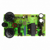
Page 30
... Board modifications Figure 23. Power transformer Delta 86H-6017 The STEVAL-ISA019V2 printed circuit board is shown in Figure 26. 30/34 Figure Doc ID 13127 Rev 4 AN2495 24, Figure 25 and ...
Page 31
AN2495 Figure 24. Silk screen (top side) Figure 25. Silk screen (bottom side) Figure 26. Copper tracks Doc ID 13127 Rev 4 Board modifications 31/34 ...
Page 32
... References 11 References ● STMicroelectronics application note AN1889 "ESBT STC03DE120 IN 3-PHASE AUXILIARY POWER SUPPLY" ● STMicroelectronics application note AN1262 "OFFLINE FLYBACK CONVERTERS DESIGN METHODOLOGY WITH THE L6590 FAMILY" ● STMicroelectronics application note AN2131 "HIGH POWER 3-PHASE AUXILIARY POWER SUPPLY DESIGN BASED ON L5991 AND ESBT STC08DE150" ...
Page 33
AN2495 12 Revision history Table 5. Document revision history Date 28-Mar-2007 10-Apr-2007 02-Jul-2007 20-May-2009 Revision 1 First issue 2 Equation 5 and Equation 15 3 ESBT part number has been updated – Section 10: Board modifications 4 – Minor text ...
Page 34
... Information in this document is provided solely in connection with ST products. STMicroelectronics NV and its subsidiaries (“ST”) reserve the right to make changes, corrections, modifications or improvements, to this document, and the products and services described herein at any time, without notice. All ST products are sold pursuant to ST’s terms and conditions of sale. ...