MULTIPHSPOL-RD Silicon Laboratories Inc, MULTIPHSPOL-RD Datasheet - Page 13
MULTIPHSPOL-RD
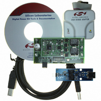
Manufacturer Part Number
MULTIPHSPOL-RD
Description
KIT REFERENCE DESIGN FOR SI825X
Manufacturer
Silicon Laboratories Inc
Type
Other Power Managementr
Specifications of MULTIPHSPOL-RD
Main Purpose
DC/DC, Step Down
Outputs And Type
1, Non-Isolated
Voltage - Output
3.3V
Current - Output
40A
Voltage - Input
10 ~ 15V
Regulator Topology
Buck
Frequency - Switching
391kHz
Board Type
Fully Populated
Utilized Ic / Part
SI8250, SI8251, SI8252
Input Voltage
10 V to 15 V
Output Voltage
3.3 V
Interface Type
USB
Product
Power Management Modules
Supply Current
10 A
For Use With/related Products
Si8250
Lead Free Status / RoHS Status
Contains lead / RoHS non-compliant
Power - Output
-
Lead Free Status / Rohs Status
Lead free / RoHS Compliant
Other names
336-1323


8.1. DPWM Timing Diagram Editor
The DPWM Timing Diagram Editor permits designers to generate DPWM initialization code by simply drawing
the timing for their end system. The wizard accommodates up to six output phases and can be used to establish
positive or negative dead-times, relative edges, absolute edges, and other timing required by the end system.
Refer to the Si825x data sheet for a description of the different edges.
This example illustrates how to use the DPWM Timing Diagram Editor to create and simulate the timing for a
single-phase POL as well as generate the initialization code in the Kernel.
1. To open the DPWM Timing Diagram Editor window, open the Application Builder and select System
2. To create an absolute edge on Phase 1, hold the mouse above the Phase 1 zero timing line (default) at time tick
3. To finish the timing for Phase 1, specify hardware modulation using (Cu0). This event edge will be modulated
1. Now, create the timing for Phase 2. For Phase 2, the goal is to create a relative rising edge relative to the falling
2. To finish the timing for Phase 2, create an absolute falling at time tick 505. To create this edge, hold the mouse
Configuration→DPWM Timing Diagram Editor from the menu.
10. Then, either double click with the left mouse button or right-click at that point and select Absolute Edge. An
absolute edge at time tick 10 will be created (see Figure 9).
relative to its absolute edge at time tick 10. To create this edge, hold the mouse above the Phase 1 timing line to
the right of time tick 10 at time tick 60. Either double-click or right-click at that point and select Event (Cu0)
Edge. Next, select the edge to reference by clicking on edge 1 in Phase 1. A relative falling (Cu0) edge will be
created at time tick 60 since u(n) defaults to 50 (see Figure 9).
edge of Phase 1 and an absolute falling edge on Phase2 at time tick 505. To create the relative rising edge,
hold the mouse above the Phase 2 zero timing line (default) at time tick 100. Then, either double-click with the
left mouse button or right-click at that point and select Relative Edge. Next, select the edge to reference by
clicking on Phase 1’s falling edge. A relative edge at approximately time tick 90 will be created (see Figure 10).
above the Phase 2 timing line at time tick 505. Then, either double-click with the left mouse button or right-click
at that point and select Absolute Edge. An absolute edge at time tick 505 will be created (see Figure 10).
Figure 9. DPWM Timing Diagram Editor—Phase 1
Confidential Rev. 0.2
Si825x Multi-Phase POL-RD
13
Related parts for MULTIPHSPOL-RD
Image
Part Number
Description
Manufacturer
Datasheet
Request
R

Part Number:
Description:
SMD/C°/SINGLE-ENDED OUTPUT SILICON OSCILLATOR
Manufacturer:
Silicon Laboratories Inc
Part Number:
Description:
Manufacturer:
Silicon Laboratories Inc
Datasheet:
Part Number:
Description:
N/A N/A/SI4010 AES KEYFOB DEMO WITH LCD RX
Manufacturer:
Silicon Laboratories Inc
Datasheet:
Part Number:
Description:
N/A N/A/SI4010 SIMPLIFIED KEY FOB DEMO WITH LED RX
Manufacturer:
Silicon Laboratories Inc
Datasheet:
Part Number:
Description:
N/A/-40 TO 85 OC/EZLINK MODULE; F930/4432 HIGH BAND (REV E/B1)
Manufacturer:
Silicon Laboratories Inc
Part Number:
Description:
EZLink Module; F930/4432 Low Band (rev e/B1)
Manufacturer:
Silicon Laboratories Inc
Part Number:
Description:
I°/4460 10 DBM RADIO TEST CARD 434 MHZ
Manufacturer:
Silicon Laboratories Inc
Part Number:
Description:
I°/4461 14 DBM RADIO TEST CARD 868 MHZ
Manufacturer:
Silicon Laboratories Inc
Part Number:
Description:
I°/4463 20 DBM RFSWITCH RADIO TEST CARD 460 MHZ
Manufacturer:
Silicon Laboratories Inc
Part Number:
Description:
I°/4463 20 DBM RADIO TEST CARD 868 MHZ
Manufacturer:
Silicon Laboratories Inc
Part Number:
Description:
I°/4463 27 DBM RADIO TEST CARD 868 MHZ
Manufacturer:
Silicon Laboratories Inc
Part Number:
Description:
I°/4463 SKYWORKS 30 DBM RADIO TEST CARD 915 MHZ
Manufacturer:
Silicon Laboratories Inc
Part Number:
Description:
N/A N/A/-40 TO 85 OC/4463 RFMD 30 DBM RADIO TEST CARD 915 MHZ
Manufacturer:
Silicon Laboratories Inc
Part Number:
Description:
I°/4463 20 DBM RADIO TEST CARD 169 MHZ
Manufacturer:
Silicon Laboratories Inc