MULTIPHSPOL-RD Silicon Laboratories Inc, MULTIPHSPOL-RD Datasheet - Page 20
MULTIPHSPOL-RD
Manufacturer Part Number
MULTIPHSPOL-RD
Description
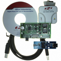
KIT REFERENCE DESIGN FOR SI825X
Manufacturer
Silicon Laboratories Inc
Type
Other Power Managementr
Specifications of MULTIPHSPOL-RD
Main Purpose
DC/DC, Step Down
Outputs And Type
1, Non-Isolated
Voltage - Output
3.3V
Current - Output
40A
Voltage - Input
10 ~ 15V
Regulator Topology
Buck
Frequency - Switching
391kHz
Board Type
Fully Populated
Utilized Ic / Part
SI8250, SI8251, SI8252
Input Voltage
10 V to 15 V
Output Voltage
3.3 V
Interface Type
USB
Product
Power Management Modules
Supply Current
10 A
For Use With/related Products
Si8250
Lead Free Status / RoHS Status
Contains lead / RoHS non-compliant
Power - Output
-
Lead Free Status / Rohs Status
Lead free / RoHS Compliant
Other names
336-1323


Si825x Multi-Phase POL-RD
10.2. Switches and LEDs
One switch is provided on the target board. Switch S1 is connected to the RESET pin of the Si8250. Pressing S1
puts the Si8250 device into its hardware-reset state.
Two LEDs are also provided on the target board. The POWER IN LED is used to indicate that the POL target board
is properly powered. The POWER GOOD LED is used to indicate that VOUT power is being regulated by the
Si8250. See Table 2 for a description of each LED and on board switches.
10.3. V
The user-provided power supply should be connected to connectors J1 and J2 where J2 is the reference. The
power source must be from 10–15 V with at least 10 A maximum output.
10.4. V
Connectors J3 and J4 are the dc output from the Si8250 Multi-Phase POL Target Board. A load (preferably
electronic) should be connected here.
10.5. V
Connectors J5 and J4 provide an alternate output monitoring note that minimizes output loading while V
being monitored.
20
IN
OUT
OUT
(J1, J2)
POWERGOOD
(J3, J4)
(J5, J4)
POWERIN
Label
RST
Table 2. Target Board Switch and LED Descriptions
Jumper #
Jumper #
Jumper #
J1
J2
J3
J4
J5
J4
Reference
LED
LED
Table 3. J1, J2 Pin Descriptions
Table 4. J3, J4 Pin Descriptions
Table 5. J5, J4 Pin Descriptions
S1
Alternate V
Confidential Rev. 0.2
Si8250 Reset Switch
Indicates that V
Indicates that V
3.3 V (Nominal), 40 A max
OUT
10–15 V, 10 A
Description
Description
Description
Sense, minimal loading
GND
GND
GND
IN
OUT
is operating properly
Description
is regulated properly
OUT
is
Related parts for MULTIPHSPOL-RD
Image
Part Number
Description
Manufacturer
Datasheet
Request
R

Part Number:
Description:
SMD/C°/SINGLE-ENDED OUTPUT SILICON OSCILLATOR
Manufacturer:
Silicon Laboratories Inc
Part Number:
Description:
Manufacturer:
Silicon Laboratories Inc
Datasheet:
Part Number:
Description:
N/A N/A/SI4010 AES KEYFOB DEMO WITH LCD RX
Manufacturer:
Silicon Laboratories Inc
Datasheet:
Part Number:
Description:
N/A N/A/SI4010 SIMPLIFIED KEY FOB DEMO WITH LED RX
Manufacturer:
Silicon Laboratories Inc
Datasheet:
Part Number:
Description:
N/A/-40 TO 85 OC/EZLINK MODULE; F930/4432 HIGH BAND (REV E/B1)
Manufacturer:
Silicon Laboratories Inc
Part Number:
Description:
EZLink Module; F930/4432 Low Band (rev e/B1)
Manufacturer:
Silicon Laboratories Inc
Part Number:
Description:
I°/4460 10 DBM RADIO TEST CARD 434 MHZ
Manufacturer:
Silicon Laboratories Inc
Part Number:
Description:
I°/4461 14 DBM RADIO TEST CARD 868 MHZ
Manufacturer:
Silicon Laboratories Inc
Part Number:
Description:
I°/4463 20 DBM RFSWITCH RADIO TEST CARD 460 MHZ
Manufacturer:
Silicon Laboratories Inc
Part Number:
Description:
I°/4463 20 DBM RADIO TEST CARD 868 MHZ
Manufacturer:
Silicon Laboratories Inc
Part Number:
Description:
I°/4463 27 DBM RADIO TEST CARD 868 MHZ
Manufacturer:
Silicon Laboratories Inc
Part Number:
Description:
I°/4463 SKYWORKS 30 DBM RADIO TEST CARD 915 MHZ
Manufacturer:
Silicon Laboratories Inc
Part Number:
Description:
N/A N/A/-40 TO 85 OC/4463 RFMD 30 DBM RADIO TEST CARD 915 MHZ
Manufacturer:
Silicon Laboratories Inc
Part Number:
Description:
I°/4463 20 DBM RADIO TEST CARD 169 MHZ
Manufacturer:
Silicon Laboratories Inc